
nanobaz
baz's nanoblog
Some photos and geekings from a scientist and all-round nerd
17 posts
Don't wanna be here? Send us removal request.
Last Seen Blogs

lizzybennets
lost again with no surprises

rwcspartacore-blog
Spartacore

author-rikimaru
Author Riki's Derps
author-rikimaru
Author Riki's Derps
author-rikimaru
Author Riki's Derps
Text
Night falls in Merrion Square
Open-air cinema showing of The Princess Bride in Merrion Square, Dublin, 2016.
#the princess bride#hello my name is inigo montoya#you killed my father#prepare to die#happenings#Dublin#ireland
1 note
·
View note
Text
Maxing out 2048
This is my girlfriend achieving the highest possible tile in the game 2048. It took a long time, and yes she did use the undo button, because otherwise this is pretty much impossible. Keep reading and you'll find out just how long it took.
131,072 is the highest possible number because all the positions on the board are full before combining the tiles. In order to get to the next number, 262,144, you would need a 5×5 grid, and in that case 262,144 would be nowhere near the maximum number possible.
When everything is full on the 4×4 grid, before starting the epic run in the gif, the biggest number is 65,536, or 2^(4×4) = 2^16. Adding all those numbers together gets us to the maximum, 2^(16+1) = 131,072. So, continuing that for a 5×5 grid, the largest number when it's full is 2^(5×5), so the maximum number is 2^(5×5+1) = 2^26 = 67,108,864.
We can also estimate how many moves it will take to get to this ultimate number. In 2048, tiles appear with values of either 2 or 4. This complicates our estimate a little since we don't know how many 2's and how many 4's have gone into making up a huge number. So let's take each of them separately to get upper and lower bounds for the number of moves required.
If we assume that all new tiles will be 2's, we can make an 8 tile with 2+2+2+2. So this will require 4 tiles, but only 3 moves, since each move adds two tiles together. For a 16 tile, it will be 2+2+2+2+2+2+2+2. We can make it a little clearer by using brackets for each tile: {[(2+2)+(2+2)]+[(2+2)+(2+2)]}. Counting the plus signs gives us 7 moves. It's pretty clear that to make a number N, we will need (N/2)-1 moves to make it, since each pair of tiles requires one plus sign between them. So that means if you're playing the 5×5 grid, you need to make 33,554,431 moves to max out the board using 2's!
We can make the same analysis using 4's: 8 = 4+4; 16 = 4+4+4+4; 32 = 4+4+4+4+4+4+4+4. Counting the plus signs again shows us that to make a number N, we need (N/4)-1 moves to make it with 4's. So, to max out the board with 4's would take 16,777,215 moves.
Now, remember 2's and 4's occur randomly. This means that there are multiple ways to make up each number, e.g. 16 = 2+2+2+2+4+4 or 2+2+4+4+4, etc. However, if we assume that 2's and 4's are equally likely to come up, we can just take the average of our two results to give us the real answer.
Therefore, the number of moves it would take for an actual game of 5×5 2048 to max out is 25,165,823. To put that in context, if you could make one move every second, and you played non-stop, with no sleep, no mistakes and no breaks, it would take you 291 days, 6 hours, 30 minutes and 23 seconds to max out the 5×5 board. For the 4×4 board, it's just under 13 hours and 40 minutes, assuming no mistakes.
Proof that averaging makes sense (and a generalisation):
To make 16, we can take 7 moves if we use only 2's, or 3 moves using only 4's. In between those extremes, each time we replace a pair of 2's with a 4, we save a move:
16= 2+2+2+2+2+2+2+2 7 moves 2+2+2+2+2+2+4 6 moves 2+2+2+2+4+4 5 moves 2+2+4+4+4 4 moves 4+4+4+4 3 moves
So, the average number of moves to make a 16 tile is 5. This makes sense, as it takes (N/2)-1 moves with 2's and (N/4)-1 moves with 4's, so the average of those two will be [(N/2-1)+(N/4-1)]/2 = (3N/8)-1. For N=16, 3(16)/8-1 = 5.
Using this for the 5×5 grid's maximum N=67,108,864, our real total number of moves is (3×67,108,864/8)-1 = 25,165,823, as before.
Finally, I did say that the next size up after 4×4 is 5×5, but the grid doesn't technically need to be square. A generalisation for an arbitrary rectangular m×n grid, gives us the maximum number N and the number of moves needed to make it:
0 notes
Text
Magnetic Levitation
This was a little demo for my 2nd year teaching laboratory (all credit to Stephen Porter, my TA!). The black disc is made from YBCO (yttrium barium copper oxide). When it's cooled by liquid nitrogen down to 78 K (-195°C), it becomes superconducting. This causes the little magnet to levitate above it due to the Meissner effect.
When a superconductor is in the Meissner state, it stops any magnetic fields from entering it. This means that they effectively become mirrors for any magnetic fields, so the little magnet sees an equal magnetic field being reflected back at it. Since like magnetic poles repel, the magnet is able to levitate above the superconductor.
The critical temperature for YBCO to become superconducting is around 93 K (-180°C), so it can easily be reached using liquid nitrogen, which is common in most labs. This means that even though it's around 200°C below room temperature, YBCO is still classed as a "high temperature" superconductor!
0 notes
Text
Enabling a new class of electronic devices
Using self-aligned nanodomain boundaries to open a charge transport gap in trilayer graphene
This shortened description of one of our papers first appeared in Photon Science Annual Report 2015, the year's "highlights reel" from the Deutsches Elektronen-Synchrotron (DESY).
Download: PDF
Trilayer graphene reveals unique electronic properties appealing for fundamental science and electronic technologies. We propose a simple method to open a charge transport gap and achieve a high on-off current ratio in Bernal-stacked trilayer graphene synthesized on vicinal SiC(001). Low-temperature measurements show that self-aligned, periodic nanodomain boundaries induce a huge charge transport gap of more than 1.3 eV at 10 K and 0.4 eV at 100 K. Our studies indicate the feasibility of creating electronic nanostructures using graphene on cubic-SiC/Si wafers.
Graphene is a single-atom-thick carbon sheet with properties unrivalled by any other known material. It will likely lead to a revolution in many areas of technology, but there are still some open questions. Ideally, graphene-based electronics would consist of just one or a few layers of graphene. The absence of an energy band gap like that of a semiconductor hampers the design of graphene-based device architectures. No gap opening in trilayer graphene with ABA (Bernal) stacking has been shown until now.
Recent theoretical works [1] show that graphene nanodomain boundaries (NBs) with a periodic atomic structure along their length can perfectly reflect charge carriers over a large range of energies. Harnessing this would provide a new way to control the charge carriers without the need to introduce an energy band gap. The main challenge is to produce self-aligned nanodomains with periodic NBs on a semiconducting substrate compatible with existing processes. We present a simple method to synthesize such a system with self-aligned periodic NBs.
In 2015 the new dynamic-XPS end-station, based on the Argus spectrometer, was finally installed on the high-brilliance soft X-ray P04 beamline at PETRA III (DESY). Users can now observe fast processes by following the evolution of photoemission core-level spectra (~ 0.1 sec/spectrum). The setup allows XPS users to observe surface modifications in real time. One can follow the relative contribution of different components during overlayer growth or interface formation by measuring core-level XPS spectra in scanning and snapshot modes in a loop. This opens a way to study dynamic processes at surfaces and interfaces and control the surface composition in real time.
By acquiring XPS spectra of the C 1s and Si 2p transitions during graphene growth on the cubic-SiC/Si wafer, we could stop the process as soon as the desired number of graphene layers was reached. To our knowledge no other beamline-endstation allows such control over layer-by-layer graphene growth. In terms of spectrum acquisition speed, photon flux, photon energy range, and photon energy resolution, for this use the dynamic-XPS is unrivalled. The developed setup helped us to optimize the synthesis of few-layer graphene samples [2].
The fabrication method uses Si-atom sublimation followed by high-temperature surface graphitization in ultra-high vacuum [3-6]. The steps of the vicinal SiC(001)/Si(001) wafers impart a preferential NB direction to the trilayer graphene. The step direction was close to [110], as Figure 1a illustrates. Scanning tunnelling microscopy (STM) studies reveal that the graphene contains nm-scale domains with boundaries elongated in one direction (Figure 1b), which is close to the step direction of the vicinal SiC(001) substrate (Figure 1a). Figure 1c shows an atomically resolved STM image containing several nm-scale domains connected to each other by the NBs.
Detailed analysis of the STM images measured near the NBs shows that, in most cases, NBs on the vicinal sample (Figure 1c) are rotated by 3.5° relative to one of the <110> directions. As Figure 1e illustrates, the asymmetric rotation of the graphene lattices relative to the NBs leads to the formation of a periodic structure along the boundaries, with a period of 1.37 nm. The periodic structure consists of distorted heptagons and pentagons (Figure 1e), which produce modulations in the atomically resolved STM image measured at the NB (Figure 1d).
ARPES measurements (Figures 1f -1g) allow us to extract information about the stacking order of the graphene. The fine structure indicates Bernal stacking, and the Dirac points are close to the Fermi level (Figure 1g). This is in full agreement with theoretical simulations for ideal trilayer graphene.
Figure 2a shows a schematic drawing of the nano-gap device. Devices with sub-30 nm nano-gap contacts were fabricated using electron beam lithography. Figures 2b and 2c show the I-V curves measured at different temperatures. The transport gap is clearly observed below 100 K but disappears at temperatures above 150 K. To obtain the exact value of the transport gap, we plotted the corresponding dI/dV curves in Figure 2d for temperatures below 150 K. Remarkably, the transport gap is approximately the same at 50 K and 10 K but substantially lower (0.4 eV) at 100 K.
We also measured I-V characteristics at 10 K with the current applied along the NBs. No transport gap was observed in this case and the I-V curve displayed nonlinear behaviour. This indicates that the charge transport gap observed for current across the NBs is mainly due to the reflection of charge carriers from the NBs.
We have proposed a new method to synthesize graphene with self-aligned periodic NBs. The vicinal SiC(001) substrates used are compatible with silicon processes. Electrical measurements show the opening of a transport gap in the graphene synthesized on this stepped surface. This development may lead to new tuneable electronic nanostructures made from graphene on cubic-SiC, opening up opportunities for a wide range of new applications.
Authors
Han-Chun Wu[1], Alexander N. Chaika[2,3], Tsung-Wei Huang[4], Askar Syrlybekov[2], Mourad Abid[5], Victor Yu. Aristov[3,6,7], Olga V. Molodtsova[6], Sergey V. Babenkov[6], D Marchenko[8,9], Jaime Sánchez-Barriga[8], Partha-Sarathi Mandal[8], Andrei Yu. Varykhalov[8], Yuran Niu[10], Barry E. Murphy[2], Sergey A. Krasnikov[2], Olaf Lübben[2], JingJing Wang[2], Huajun Liu[11], Li Yang[12], Hongzhou Zhang[2], Mohamed Abid[5], Yahya T. Janabi[13], Sergei N. Molotkov[3], Ching-Ray Chang[4], and Igor Shvets[2]
School of Physics, Beijing Institute of Technology, Beijing 100081, People’s Republic of China
CRANN, School of Physics, Trinity College Dublin, Dublin 2, Ireland
Institute of Solid State Physics RAS, Chernogolovka, Moscow district 142432, Russian Federation
Department of Physics, National Taiwan University, Taipei 10617, Taiwan
KSU-aramco Center, King Saud University, Riyadh 11451, Saudi Arabia
Deutsches Elektronen-Synchrotron DESY, 22607 Hamburg, Germany
Institut für Theoretische Physik, Universität Hamburg, Jungiusstrasse 9, D-20355 Hamburg, Germany
Helmholtz-Zentrum Berlin für Materialien und Energie, D-12489 Berlin, Germany
Freie Universität Berlin, D-14195 Berlin, Germany
MAX-lab, Lund University, Box 118, 22100 Lund, Sweden
Institute of Plasma Physics, Chinese Academy of Sciences, Hefei 230031, People’s Republic ofChina
Electronic Engineering Institute, Hefei 230037, People’s Republic of China
Saudi Aramco Materials Performance Unit TSD, Research & Development Center, Dharhan 31311, Saudi Arabia
Original publication
“Transport Gap Opening and High On-Off Current Ratio in Trilayer Graphene with Self-Aligned Nanodomain Boundaries”, ACS Nano 9, 8967–8975 (2015).
DOI: 10.1021/acsnano.5b02877
References
O. V. Yazev and S. G. Louie, “Electronic Transport in Polycrystalline Graphene”, Nat. Mater. 9, 806 (2010)
Sergey V. Babenkov, et al, “A new dynamic-XPS end-station for beamline P04 at PETRA III/DESY”, NIM in Physics Research A 777, 189 (2015)
V.Yu. Aristov, et al, “Graphene synthesis on Cubic SiC/Si wafers. Perspectives for mass production of graphene-based electronic devices”, Nano Letters 10, 992 (2010)
Alexander N. Chaika, et al, “Continuous wafer-scale graphene on cubic-SiC(001)”, Nano Research 6, 562 (2013)
Alexander N Chaika, et al, “Rotated domain network in graphene on cubic-SiC(001)”, Nanotechnology 25, 135605 (2014)
A. N. Chaika, et al, “Fabrication of [001]-oriented tungsten tips for high resolution scanning tunnelling microscopy”, Scientific Reports 4, 3742 (2014)
0 notes
Photo
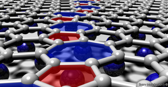
Stepping Stones
Two perfect honeycomb domains of graphene meet at an angle. This angle isn't the ideal 60°, so the hexagons at the border distort into pairs of pentagons and heptagons. The 5- and 7-sided rings bond the two lattices like a zipper. They form a periodic pattern that changes the properties of the whole single-atom-thick layer.
nanobaz.com
0 notes
Link
Video Credit: Nate J Cira and Manu Prakash, Stanford University Surface tension lies behind these beautiful interactions between liquid droplets. For more in...
0 notes
Photo

Laser-cut slate Game of Thrones sigil coasters from http://www.etsy.com/ie/shop/TheHoneycombAdam
2 notes
·
View notes
Photo
SCIENCE!
Low energy electron diffraction image of the iconic Si(111) 7x7 surface - misaligned though
0 notes
Link
"Filamental Vortex Loops," such as those found in smoke rings and mushroom clouds, crop up in a number of applications in fluid dynamics. Earlier this year, scientists created a long-sought twist on this phenomenon: knotted vortex loops.
Really interesting video showing rings of bubbles (like smoke rings) being tied in different types of knots. I love the 3D images of the rings - now I want my own scanning laser tomograph!
More details in this video!
0 notes
Video
youtube
I found a honey bee on the windowsill and very near death, so I took him outside and have him some honey to rejuvenate him. Minutes later he was back to full health and flew off!
2 notes
·
View notes
Photo
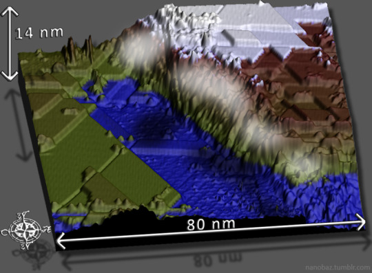
Nano-landscape
The scale bars are correct, the clouds were added later!
The nano-scale world mirrors the macro-scale. This is a valley and plateau more than 1000 times smaller than the width of a hair, on the surface of a silver crystal, imaged by scanning tunneling microscope.
The small hillocks are the height of a single atom and the “waves” in the sea are actually individual molecules which self-assemble into ordered structures.
The study of such self-organisation is key for the future of electronics, which may be made up of circuits comprised of single molecules.
0 notes
Photo

Abigail the bichon yorkie loves to play
0 notes

Photo

Rainy old Ireland
I like how the grooves in the decking form a Moiré pattern with the pixels in the camera
1 note
·
View note
Photo

Stream in the Blackstairs Mountains
0 notes