#2nm chip
Text
Samsung Electronics Targeting Mass Production of 2nm Chips by 2025, 1.4nm by 2027
Samsung Electronics Targeting Mass Production of 2nm Chips by 2025, 1.4nm by 2027
Samsung’s chip contract manufacturing business said on Tuesday it plans to more than triple its advanced chips production capacity by 2027 to meet strong demand despite current global economic headwinds.
The world’s second-largest foundry after Taiwan Semiconductor Manufacturing Co (TSMC) is targeting mass production of advanced 2-nanometre technology chips by 2025 and 1.4-nanometre chips by…

View On WordPress
0 notes
Text
2nm chip for iPhone 17 Pro on track despite twin challenges - 9to5Mac
2nm chip for iPhone 17 Pro on track despite twin challenges 9to5Mac http://dlvr.it/T5w9Pj
0 notes
Text
AMD Zen 6: Release Date, Specs & Everything We Know So Far
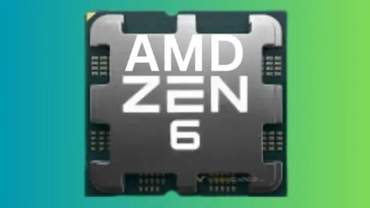
AMD Zen 6 Roadmap
While the world awaits AMD’s Zen 5 architecture, tech industry rumors of AMD Zen 6 are beginning to circulate. Zen 6 will revolutionize performance and efficiency when it launches in 2025 or 2026. See what this next-generation architecture will bring.
A Manufacturing Advancement
A Step Forward in Manufacturing there are rumor’s that AMD Zen 6 will use the cutting-edge 2nm or even 3nm process nodes from TSMC. This would be a substantial leap from the 5nm node that was predicted for AMD Zen 5. As a result of this miniaturisation, it is possible to pack a greater number of transistors into the same overall size, which may result in potential performance benefits and increased power efficiency.
Core Count Dilemma
Conundrum regarding Core Count there are rumor’s that suggest there could be three different types of AMD Zen 6 Standard, Dense Classic, and Client Dense. It is anticipated that the Standard variation would be the flagship edition, as it will provide the greatest clock rates for desktop computers. In order to improve efficiency, the Dense Classic may be designed to meet the needs of servers by providing a greater number of cores per chiplet at lower clock speeds. There is still a lot of uncertainty around the Client Dense variation, although there are rumors that it would be aimed at mobile devices and laptops. It would prioritise even lower core sizes, but it might sacrifice some speed in the process.
Improvements to the Instruction Set
Improvements to the Instruction Set It is quite likely that AMD Zen 6 will include a new instruction set, which will likely expand upon the basis that Zen 5 established. This could involve CPU optimisations for certain workloads like machine learning (ML) and artificial intelligence (AI), which would further boost the processor’s capabilities in these quickly expanding domains.
Integrated Visualisation is Growing
Integrated Graphics on the Rise talk of AMD Zen 6 possibly moving directly to RDNA 5 for its integrated GPUs (iGPUs), eschewing RDNA 4 entirely. This could result in significant performance increases for integrated graphics, which would make them more viable solutions for gamers who play games on a casual basis and for jobs that are performed typically.
Enhanced Delivery of Power
An increase in power delivery the power requirements of AMD Zen 6 processors are expected to increase in tandem with the potential for an increase in core counts and clock rates. The implementation of enhanced power supply methods, which may include the incorporation of 2.5D chip connection technologies, will be essential for the preservation of both stability and efficiency.
Compliance with Sockets
In terms of compatibility with sockets, there is a possibility that AMD Zen 6 would introduce a new socket, which would necessitate an upgrade to the motherboard in order to ensure compatibility. Nevertheless, a few leaks indicate that it might still make use of the AM5 connector, which Zen 4 introduced, providing some backward compatibility.
Fighting for Domination
The struggle for domination AMD and Intel are in a very competitive market. With its forthcoming architectures, Intel is also pushing the envelope, but AMD Zen 6 might make AMD even more of a leader in high-performance computing.
Anticipating the Unknown
The wait for the unknown information is still being withheld, despite the positive impression that leaks and rumours provide. When it comes to validating these rumours and offering a more accurate picture of AMD Zen 6‘s capabilities, official information from AMD will be absolutely necessary.
Past the Specification Sheet
In addition to the Spec Sheet the ultimate impact of AMD Zen 6 will go beyond the characteristics that it possesses in their raw form. This has the potential to make it:
AMD Zen 6 has the potential to revolutionise the gaming experience because to its increased performance and the possibility of more powerful integrated graphics processing units (iGPUs).
In order to empower content creators, faster processing and greater efficiency could be of significant use to content creators who deal with applications that are demanding.
Increase the speed of artificial intelligence and machine learning optimization’s for workloads in AI and ML could open up new opportunities for academics and developers working in these areas.
The introduction of AMD Zen 6 symbolises the beginning of an exciting new phase in the development of CPUs. The prospective advantages in performance and efficiency promise to make the wait worthwhile, despite the fact that it may appear to be a lengthy period of time. As more information becomes available, people can anticipate that the excitement surrounding AMD Zen 6 will continue to grow, leaving all of us excited to witness the arrival of this next-generation design.
AMD Zen 6 release date
The AMD Zen 6 processors have no official release date as of now. The following is what we know from leaks and rumors:
Potential Finalization: Rumor has it that AMD plans to complete the Zen 6 product design by Q3 2024, or sometime in September.
Possible Delay: Nevertheless, certain sources indicate that because of doubts over the production procedures, the release may be pushed back to 2026.
All things considered, it seems unlikely that AMD Zen 6 processors will be released before late 2025, if at all. Keep an eye on Govindhtech news websites or AMD for any official announcements.
Read more on govindhtech.com
0 notes
Text
TSMC secures more $11 Billion Funding As per the Chips Act, so that 2nm nanosheet production by 2028
#TSMC
#CHiPs
#TechNews
#TechTrends
#TECH4ALL
#TechInnovation
#TechnologyNews

0 notes
Text
TSMC 2nm Trial Production To Begin in 2024; HVM by 2025 - techovedas
0 notes
Link
0 notes
Text
U.S. Welcomes TSMC's Advanced Chip Tech
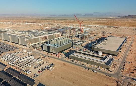
The Biden-Harris Administration and TSMC Arizona ink a deal for up to $6.6 billion in CHIPS funding, enabling TSMC's $65 billion investment in Arizona for the world’s most advanced semiconductor fabs. This partnership promises to bolster U.S. tech leadership, economic, and national security through cutting-edge 2nm chip technology.
The Groundbreaking Agreement
Under the illuminated skies of innovation and progress, the preliminary memorandum of terms inked between the U.S. Department of Commerce and TSMC Arizona heralds a new era.
With up to $6.6 billion in proposed CHIPS Direct Funding, TSMC announces its commitment to bring 2 nanometer technology to its second fab and a new third fab dedicated to producing 2 nanometer or more advanced chips.
This ambitious initiative, part of a more than $65 billion investment, sets the stage for the U.S. to host the world's most advanced semiconductors, right in the heart of Phoenix, Arizona.
Strengthening Economic and National Security
The Biden-Harris Administration's foresight in solidifying the U.S.'s semiconductor supply is a masterstroke in economic and national security strategy.
By anchoring the production of cutting-edge chips domestically, the initiative not only mitigates vulnerabilities but also propels the U.S. back to the forefront of global semiconductor manufacturing.
The promise of creating approximately 6,000 direct manufacturing jobs, alongside tens of thousands of indirect employment opportunities, sketches a vibrant economic future for Arizona and the nation at large.
Powering the Future: AI and Beyond
At the heart of this technological renaissance is the development and application of 2nm technology, a marvel in semiconductor manufacturing.
This leap forward is critical for powering next-generation AI, high-performance computing, and 5G/6G communications. TSMC's expansion in Arizona is a testament to the U.S.'s commitment to not just participating in the global tech race but leading it.
The foresight to house such advanced manufacturing capabilities domestically underscores a strategic move towards securing technological sovereignty and a competitive edge in critical future-facing industries.
Community Impact and Workforce Development
Beyond the silicon and circuits, the TSMC investment is a catalyst for community transformation and workforce development. The proposed funding includes dedicated efforts towards nurturing a skilled workforce capable of steering the future of semiconductor manufacturing.
Partnerships with local educational institutions and training programs promise not only job creation but also a sustainable talent pipeline equipped to tackle the challenges of tomorrow's tech landscape.
Reflections on a Tech-Forward Future
As we stand on the brink of this new technological frontier, it's clear that the TSMC investment is more than an economic booster; it's a cornerstone in the U.S.'s journey towards reclaiming its status as a global leader in tech innovation.
The initiative's ripple effects—spanning economic revitalization, technological advancement, and enhanced national security—paint a promising picture of the future.
The Road Ahead
The TSMC-Arizona partnership is a powerful symbol of American ingenuity and a blueprint for future success. However, this is just the beginning. To fully capitalize on this opportunity, the United States must:
Double down on STEM education: We need to inspire the next generation of engineers and scientists to ensure a talent pipeline that can sustain this technological resurgence.
Foster a collaborative ecosystem: Collaboration between industry, government, and academia is crucial to accelerate innovation and maintain a competitive edge.
Invest in research and development: Continued investment in R&D is vital to push the boundaries of technology and ensure American leadership in future chip generations (beyond 2nm).
By taking these steps, the United States can solidify its position as a global technology leader, reaping the economic and security benefits for decades to come.
The future is bright, but continued focus and investment are necessary to turn the promise of this partnership into a reality that benefits all Americans.
Sources: THX News & US Department of Commerce.
Read the full article
#5G/6Gcommunications#advancedchipstechnology#AIandcomputing#Arizonatechhub#Biden-HarrisAdministration#CHIPSandScienceAct#nationalsecurity#SemiconductorManufacturing#TSMCArizonaCorporation#U.S.economicsecurity
0 notes
Text
The Race to 2nm: RISC-V Chips in Japan – By Dr. Ian Cutress
https://morethanmoore.substack.com/p/the-race-to-2nm-risc-v-chips-in-japan
0 notes
Link
Apple has started designing 2nm chips for future iPhone models
0 notes
Link
Samsung and TSMC will continue to produce 2nm chips in Taiwan and Korea - technology - https://newtechmania.com/samsung-and-tsmc-will-continue-to-produce-2nm-chips-in-taiwan-and-korea-technology/
0 notes
Text
Report: TSMC and Samsung to Keep 2nm Chip Production in Taiwan, Korea | Extremetech
0 notes
Link
Theo Gizmochina, thông tin này được CEO Intel Pat Gelsinger xác nhận trong thông báo mới đây, cho biết công ty ông có thể vượt qua tốc độ của Định luật Moore vào năm 2031 và hướng đến khái niệm mới gọi là "Định luật Super Moore", hay "Định luật Moore 2.0", vì số lượng bóng bán dẫn tăng lên. TSMC và Samsung Foundry sẽ đóng một vai trò đặc biệt trong việc hỗ trợ Intel trong sản xuất chip mới dựa trên tiến trình 2nm. Ngay cả Qualcomm cũng đang chuyển sang TSMC và Samsung Foundry.CEO Intel Pat Gelsinger đặt mục tiêu lớn cho Intel vào năm 2030Chia sẻ trong buổi trò chuyện của mình, Gelsinger cho biết: "Tôi nghĩ chúng ta đã tuyên bố về cái chết của Định luật Moore trong khoảng ba đến bốn thập kỷ. Mặc dù điều đó có thể đúng, bởi chúng ta không còn ở kỷ nguyên vàng của Định luật Moore nữa. Giờ đây nó khó hơn rất nhiều, vì vậy có lẽ chúng ta chỉ có thể thực hiện việc tăng gấp đôi mật độ bán dẫn sau mỗi ba năm, chậm hơn so với hai năm như định luật đã nêu. Nhìn chung, tốc độ đã chậm lại".Bất chấp tốc độ chậm nhưng Gelsinger tin tưởng Intel có thể đạt được con số kỳ diệu 1.000 tỉ bóng bán dẫn trên một con chip vào năm 2030. Đây không phải là lần đầu tiên một quan chức công ty đề cập đến bước phát triển lớn như vậy. Ngay cả Phó chủ tịch điều hành kiêm Tổng giám đốc Bộ phận Phát triển Công nghệ của Intel, Ann Kelleher, cũng tiết lộ: "Khi Định luật Moore ngày càng phát triển, tốc độ truyền thống đang chậm lại".Có một số công nghệ khác nhau có thể giúp Intel đạt được mốc 1.000 tỉ bóng bán dẫn cho một con chip. Công ty đặt mục tiêu thực hiện việc đóng gói tiên tiến và tích hợp không đồng nhất để đóng gói nhiều bóng bán dẫn hơn vào một con chip. Ngoài ra, công ty có kế hoạch sử dụng công nghệ RibbonFET mà Samsung sử dụng để sản xuất chip 3nm. Đó là công nghệ bao phủ cả bốn phía giúp giảm rò rỉ dòng điện. Ngoài ra, một cách khác mà Intel có thể đạt được là thông qua PowerVIA Power Delivery với mục đích di chuyển các đường cấp nguồn ra phía sau chip nhằm cải thiện hiệu suất.Tuy nhiên, những tiến bộ này sẽ khiến Intel phải trả giá rất nhiều. Gelsinger cho biết:"Bảy hoặc tám năm trước, một nhà máy hiện đại sẽ có giá khoảng 10 tỉ USD. Nhưng giờ đây, nó trị giá khoảng 20 tỉ USD. Vì vậy chúng ta đã thấy một sự thay đổi rõ rệt về kinh tế".
0 notes
Text
Intel’s AI-Centric Advances: Impact on CPUs and Cloud Services
AI Integration in High-End Processors: Intel’s Meteor Lake CPUs and Server Offerings
In a landscape increasingly dominated by the artificial intelligence (AI) revolution, semiconductor giant Intel has strategically positioned itself at the forefront. This strategic move is evident in their latest offerings, such as the Meteor Lake CPUs, which go beyond traditional processing capabilities. These CPUs feature built-in hardware specifically designed for local AI inference workloads in the PC market. Notably, functions like background blurring in video conferencing can be offloaded to dedicated AI hardware. This not only enhances user experiences but also optimizes the CPU and GPU for other processing tasks, resulting in a faster overall performance and improved battery life for devices.
A parallel initiative is observed in the server market, where Intel’s Sapphire Rapids and Emerald Rapids server CPUs come equipped with AI accelerators. While these CPUs may not match the efficiency of high-powered GPUs, they present a cost-effective solution, especially in light of the increasing rarity and cost of data center GPUs. Intel’s focus on reducing the total cost of ownership is a strategic move aimed at appealing to a broad range of customers.
Competition in the AI Accelerator Space: Intel’s Gaudi Line vs. NVIDIA
The competitive landscape in the high-end processor market intensifies as Intel directly challenges NVIDIA with its Gaudi line of AI accelerators. The latest iteration, Gaudi2, though not as powerful as NVIDIA’s top-tier products, delivers commendable performance. The imminent launch of Gaudi3 later this year further positions Intel as a formidable alternative in the AI accelerator space. This competition is vital for driving innovation and providing consumers with diverse, high-performance options for AI-related workloads.
Semiconductor Manufacturing Advancements: Intel’s Foundry Business and High-NA EUV Machines
Intel’s commitment to staying at the forefront of semiconductor manufacturing is showcased through its foundry business. The rapid rollout of new process nodes, with Intel 4 in mass production and Intel 3 arriving early this year, positions Intel as a key player for AI chip designers seeking advanced manufacturing capabilities. Notably, Intel’s plans for High Numerical Aperture (High-NA) EUV machines signify a pivotal advancement. These machines, with 0.55 numerical aperture optics, are critical for enabling nodes below 2nm/20 angstroms. While High-NA machines won’t be part of the production plans for the upcoming 18A node, they will play a crucial role in Intel’s post-18A node production, referred to as “Intel Next.”
Creation of Articul8: Intel’s Strategic Move into Enterprise AI
Intel’s strategic partnership with digitalbridge has led to the establishment of Articul8, an independent AI company. This move signals Intel’s commitment to expanding its footprint in the AI landscape. Articul8’s platform, optimized for Intel’s server CPUs and Gaudi accelerators, resembles IBM’s WatsonX, indicating a recognition of specific enterprise needs for deploying AI technology. The platform’s focus on security aligns with industry trends, particularly in highly regulated sectors like financial services, where data privacy is paramount.
Intel’s equity stake in Articul8, along with other venture investors, exemplifies a strategic approach to external capital utilization. This strategy allows Intel to refocus its resources on core businesses while maintaining a stake in a promising venture that aligns with its broader objectives. Such moves are not unprecedented for Intel, which previously sought external capital for its automotive chip subsidiary, Mobileye, and spun off its Programmable Solutions group into a standalone business.
Implications for Cloud Service Providers: Enhanced AI Capabilities and Efficiency
As Intel solidifies its position in the AI landscape, cloud service providers are poised to reap the benefits. The integration of AI capabilities into Intel’s processors, coupled with advancements in semiconductor manufacturing, holds significant implications for high-end processor competition. Cloud providers stand to gain from improved AI capabilities, potentially leading to more sophisticated and efficient services. The appeal of Intel’s AI-enabled chips for infrastructure in the cloud service sector is likely to grow, providing a robust foundation for enhanced AI-related workloads and services.
Conclusion
Intel’s strategic focus on AI integration and semiconductor advancements underscores its commitment to staying competitive in the rapidly evolving technology landscape. The implications extend beyond direct competition with industry players, impacting the broader ecosystem, including cloud service providers set to capitalize on enhanced AI capabilities and efficiency.
Source:
https://biz.crast.net/intel-has-found-another-way-to-win-in-the-ai-market-3/
https://www.anandtech.com/show/20066/intel-highna-lithography-update-dev-work-on-intel-18a-production-in-future-node
https://www.anandtech.com/show/21194/asml-ships-first-high-na-euv-scanner-to-intel
This article is re-published from: https://www.scloud.sg/resource/intel-ai-centric-advances-impact-on-cpus-and-cloud-services/
0 notes
Last Seen Blogs

berlinsagger
ButtcrackBoy

fayrithh
BooBoo Za Fool

thorsdiana
heart and soul

eccentricalli
Blue Sky Thinking

wisebreadsong
Senza titolo