
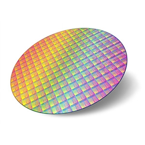
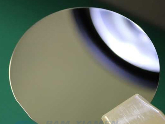
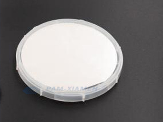
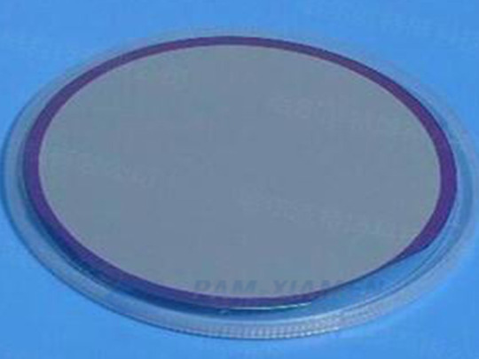
ganwafer
Xiamen Powerway Advanced Material Co., Ltd
Xiamen Powerway Advanced Material Co., Limited (PAM-XIAMEN) is a top-class enterprise for compound semiconductor material integrating semiconductor crystal growth, process development, and epitaxy.
19 posts
Don't wanna be here? Send us removal request.
Last Seen Blogs

stoenhearts
everything enthusiast

fleurdelissaswords-blog
Fleur De Lissa & Tupeck the Rapping Parrot's World

tvguidechanandlerbong
For All My Random Stoner Crap

tamirismonique
Tamiris Brito

orionkeptmeburning-blog
I love kawaii things // Hiatus until 26/12
Text
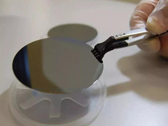
Epitaxy and the Process of Epi Wafer Manufacturer
For silicon wafer processing a wafer needs to meet certain quality specifications, like chemical, mechanical, surface specifications, and electrical specifications. It is important that Epi wafer undergo these quality criteria so a wafer is marked as defect-free and of excellent quality. For different electronic applications, there is the use of high-quality wafers in semiconductor manufacturing. To guarantee that the devices produced are efficient it goes through a series of thorough processing, including epitaxial growth. This article depicts epitaxial growth and its significance in manufacturing semiconductors.

Epitaxial Growth or Epitaxy
Epitaxy plays an important role in silicon wafer processing for semiconductor applications. Epitaxial growth or epitaxy is a process in which over a single crystal substrate a fine layer of single-crystal material is transferred along with the help of chemical vapor deposition. Epitaxy is performed to boost and develop the performance of bipolar devices. It helps in giving good control to the doping concentration of the devices, therefore making the layers oxygen and carbon-free. An example is the deposition of silicon over a silicon substrate. Epi wafer suppliers are present everywhere to supply good quality wafers.
Silicon Wafer Processing
In producing high-quality wafers meticulous and thorough silicon wafer processing plays a huge role. We provide premium quality wafers at an affordable price at wafer world.
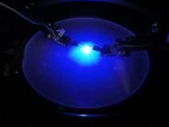
Finishing of the Process
With the use of an epitaxial reactor, the chemical vapor deposition of epitaxial growth is attained. It consists of a quartz reaction where a susceptor is placed. To the wafers, the susceptor provides mechanical support and with thermal distribution, it creates an environment. At high temperatures, an epitaxial deposition is performed which allows gasses to flow into the chamber. In Silicon epitaxy, it is observed that over thickly-doped silicon substrate there is the involvement of growing a thinly doped epi layer. Across the collector-substrate junction, this is done to achieve a higher disintegration voltage along with keeping low collector resistance. A higher operating speed is permitted by a lower collector resistance by using the same level of current. From Epi wafer manufacturer you can easily manufacture wafers according to your requirements.
Main source: https://ganwafer.mystrikingly.com/
#epi wafer#epi wafer manufacturer#epi wafer supplier#epi wafer wholesale#epi services china#epi services
1 note
·
View note
Text
Know the Future of SiC Semiconductors
Know the Future of SiC Semiconductors
From the past three years, in terms of semiconductor technology, SiC wafer has grown to such a level that it can compete with silicon. Now when it is in the 3rd generation, SiC is delivering performance with a growing number of applications.
In Today’s time, with the help of silicon carbide gems are prepared which becomes difficult to distinguish from diamond, and then it becomes even more…

View On WordPress
1 note
·
View note
Text
Get to Know Which Substrate is better for GaN Template
Get to Know Which Substrate is better for GaN Template
Today every device has begun to network as a result there is a need for speed that is ultimately pushing the industry toward 5G. It is the next-generation telecom standard that promises to give greater bandwidth and reduced latency. Many 5G bands are based on the frequency bands that are quite challenging for traditional semiconductor devices that are based on silicon GaN Epi on…
View On WordPress
#GaN epi on sapphire china#GaN epi on sapphire wafer#GaN epi on sapphire wafer manufacturer#GaN epi wafer on sapphire
1 note
·
View note
Text
Availability of High Quality GaN Substrates for Modern LED Technology
Availability of High Quality GaN Substrates for Modern LED Technology
There is the availability of both GaN templates and AlN templates. To grow 2D transition metal dichalcogenides and measure their electrical properties researchers make use of the templates. The templates are insulating along with providing negligible electrical mobility. This makes sure that the spurious electrical signal is not directed to the 2D materials on the surface.
Everyone knows the…
View On WordPress
1 note
·
View note
Text
Use of Wafer Front End in the Semiconductor Manufacturing Process
When the process of front-end production is completed then to save the chip the wafers are transmitted to the assembly facility. It brings the heat from the devices, assists the integration into the electronic systems, and confines the electric interference.
Building of wafers
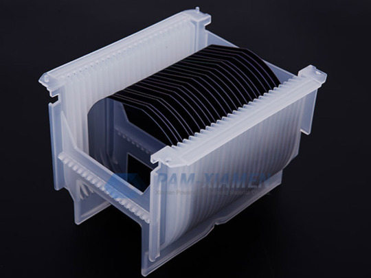
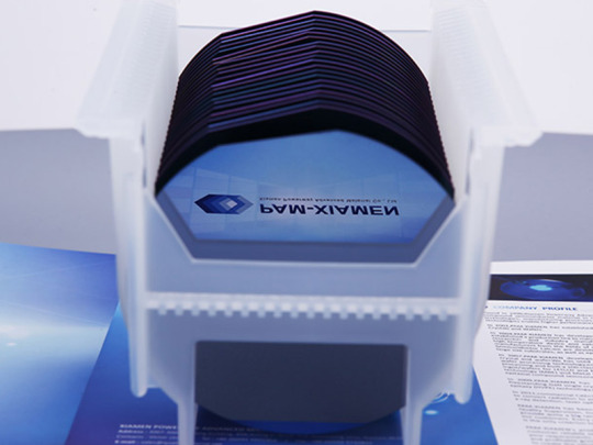
In manufacturing, the semiconductor has an essential role no matter whether it is a small chip or a big motor car. In semiconductor production, the processing of chemical elements is done in the wafer form. Within the plastic cassettes, the LED Epi wafer is built up and with the specific production time, the circumstances are made out of steps.
Wafer handling equipment is the emerging manufacturing process that is made to check the cleanliness and environmental control. Within the semiconductor front-end industry, it has diminished from the semiconductor devices manufacturing. For the significant environments, the process is carried out where certain factors are checked out, such as humidity, particle contamination, temperature, and controlled with the particular parameters.
To handle delicate thin wafers the bonding of the device wafer is done with a rigid carrier substrate before the back-thinning process. With the use of an adhesive bonding layer, the originally thick device wafer is bonded with its active surface to a carrier wafer.
It arrives in a consignment production form if we discuss the semiconductor backend production that is based on many customers' various orders. Picked up from the GaN LED wafers conveyed from the front-end production, the backend companies with the non-defective dies start building the final product in such a case. It makes the products reach their place within the due dates.

LED epitaxial wafer gives a detailed description of the non-repairable chips that are pushed to the next step. The defectiveness and the opposed information are filled up when this test gets completed and based on the matter it is passed through the backend process. The information conveys that only non-defective dies are taken in the final product. Wafer handling equipment is the emerging manufacturing process that is made to check the cleanliness and environmental control. Within the semiconductor front-end industry, it has diminished from the semiconductor devices manufacturing. The manufacturers, as with the bump in the semiconductor's request, turn on a further note towards automating the production process.
Original source: https://ganwafer.weeblysite.com/
3 notes
·
View notes
Text
Importance of Wafer Bonding in Today’s World
Wafer bonding is a phenomenon wherein at room temperature; mirror-polished, flat, and clean wafers of any material are brought in contact get attracted to each other by forces and adhere or bond. Wafer bonding is also known as direct bonding or fusion bonding. In maximum situations, the wafers that are included in actual applications are compound semiconductor wafers that consist of single-crystal materials such as silicon or gallium arsenide that are used in microelectronics or optoelectronics. When compared with that of covalently or ionically bonded solids the bonding at room temperature is usually weak. So for many applications, to strengthen the bonds across the interface the room-temperature-bonded wafers have to undergo heat treatment. Then one of the two wafers is thinned down to a thickness that may be in the range of many microns down to a couple of nanometers but depending on the specific application.
Today you will find that the most prominent applications of compound semiconductor wafer bonding are in the areas of silicon-on-insulator (SOI) devices and silicon-based sensors and actuators. SOI structures generally consist of a thin, top layer of single-crystal silicon, a layer of silicon dioxide (SiO2), and a silicon handle substrate that provides mechanical support. When the fabrication of SOI substrates is performed by wafer bonding, the silicon wafer that forms the top layer needs to be oxidized before bonding, and after bonding it needs to be thinned down to between 0.1 and 10 μm. When compared to devices on conventional silicon substrates, SOI devices that give hard radiation can operate at high temperatures and also have potentially higher packing density and lower power consumption.
Even after the dominance of silicon-related applications, wafer-bonding technology is by no means restricted to silicon wafers. Because of proper polishing and control of the chemistry of the surfaces, it has become possible to bond a variety of solids independently of their lattice parameter, structure (amorphous, polycrystalline, single-crystal), their crystallographic orientation, and or the thickness of the wafers. Hence, compound semiconductor wafer China bonding allows the fabrication of material combinations that were previously ruled out by most materials scientists, solid-state physicists, and electrical engineers, because by the conventional approach of epitaxial growth these material combinations were not possible.
Main source: https://ganwafer.wordpress.com/
#compound semiconductor wafer manufacturer#compound semiconductor wafer supplier#compound semiconductor substrate#compound semiconductor wafer china
3 notes
·
View notes
Text
Get To Know All about Wafer handling
Get To Know All about Wafer handling
By market researchers, the market potential for ultra-thin wafers, GaN wafer with backside metallization is estimated to be above 40% of the wafer market by the year 2010.
Wafer handling
To handle delicate thin wafers the bonding of the device wafer is done with a rigid carrier substrate before the back-thinning process. With the use of an adhesive bonding layer, the originally thick device…

View On WordPress
2 notes
·
View notes
Text
Use of Silicon Wafers inside the IC's
Use of Silicon Wafers inside the IC’s
From the past few decades, we have been observing that scientists have managed to introduce lots of things to the world which we can use to improve our lifestyle much better. One of the most important inventions made by these scientists is the electronic circuit system and today at most of our domestic and commercial activities we use these electronic circuits.
Whenever we discuss the electronic…
View On WordPress
2 notes
·
View notes
Text
Tips on How to Pick a Silicon Wafer supplier
For your substrates needs, it becomes difficult in finding the right supplier and custom wafers. Empathy is something that you need in your supplier along with your budget constraints.
Selecting a Silicon Wafer supplier

Electronic devices have changed the way we are living because as humans they have aided in maximizing our capabilities. Every day computers are becoming better and with the improvement of the existing systems, smartphones are changing the dynamics of information flow or cash transfer. Transport has been boosted because of the introduction of automotive electronic devices that make cars study their surroundings and respond appropriately. This has resulted in the development of drones, self-driving cars, and electric vehicles. From the use of silicon wafers to make various devices the medical industry, military, or manufacturing industry among other various fields have been benefited.
There is a need for Etching, Edge Profiling, Lapping or Grinding, Polishing, Laser Inspection, Cleaning, Wire Sawing in packaging applications of electronic devices to meet a specific application. The number of integrated circuits that can be fabricated from a wafer is determined by the surface area of a wafer. On the other hand, with the increased surface area, the cost of making the wafers also increases; however, the cost increase is not proportional to the surface area. There are different capacities for different custom wafers manufacturers so one should inquire if the desired specifications can be achieved or not.
In reducing the cost of making many wafers the number of dies that can be obtained from a wafer needs to be more. Consideration of the nature in which the atoms of silicon are aligned has to be made as it does affect the structural and electronic characteristics of a device. Every day computers are becoming better with the improvement of the existing systems. The path of the transporting ions can be determined if you consider the orientation of silicon crystal. In supplying the orientation information of the silicon wafers procured, you will find some custom wafers supplier who has to be ready. If there is any type of requirement, such suppliers are the correct choices.
Original source: https://ganwafer.mystrikingly.com/
4 notes
·
View notes
Text
Get To Know about the Wafer fabrication
We have to acknowledge that silicon is used to make semiconductor wafers - an element making up almost 30% of the crust of Earth. Constituting the basic structure of the whole semiconductor chip, it is the raw material and is responsible for its optimum functioning. Silicon has the property to control resistivity based on dopants Rather than being a very good conductor of electricity. Before a semiconductor can be built on it, this silicon material has to be turned into a wafer. This means that on this tiny piece of a pure, crystal of silicon wafer, the entire wafer fabrication process for creating the rest of the integrated circuit that will ultimately be a larger electronic device component rests.
Examples include the production of microprocessors for computers, LEDs, radio frequency (RF) amplifiers, and optical computer components. To build components with the necessary electrical structures, Wafer fabrication is used.
With electrical engineers, the main process begins designing the circuit. Defining its functions, specifying the voltages, inputs, signals, and outputs needed. Into electrical circuit design software, these electrical circuit specifications are entered similar to ones used for computer-aided design and then imported into circuit layout programs. For the layers to be defined for photomask production, this is necessary. With each step in design, the resolution of the circuit increases rapidly as the scale of the circuits is already being measured in fractions of micrometers at the start of the design process. Thus, each step for a given area increases circuit density during wafer fabrication China.
The silicon wafers start pure and blank. In layers in clean rooms, the circuits are built. First, in micrometer detail onto the wafers' surface, photoresist patterns are photo-masked. To short-wave ultraviolet light, the wafers are then exposed and the unexposed areas are thus cleaned and etched away. On to the desired zones, hot chemical vapors are deposited and baked in high heat, which into the desired zones, permeate the vapors.
Depending on the complexity of the desired connections and circuit, these steps are repeated many hundreds of times often by the wafer fabrication companies.
Main source: https://ganwafer.wordpress.com/
4 notes
·
View notes
Text
The Ingot Growth of Production Process of Silicon Wafer
The Ingot Growth of Production Process of Silicon Wafer
In modern technology, Semiconductors are extremely central and critical components. On these integrated circuits that are housed on silicon wafer chips, Most of the electronic devices we use today operate. It does, however, to get the semiconductor in that condition from the raw material, takes a lot of processing and work. The silicon wafer chip is the basic substrate of these microchips upon…
View On WordPress
4 notes
·
View notes
Text
Facts and Overview of Semiconductor Wafer
Facts and Overview of Semiconductor Wafer
In our daily life, a semiconductor wafer is invisible absolutely but in each and every electronic device we use, it exists in a form of an IC or an ASIC. Consisting of silicon dies, a Semiconductor wafer is a round piece of silicon that is designed for performing a very specific function. But you should know that there are many other interesting facts about semiconductor wafers.
Silicon is used…
View On WordPress
3 notes
·
View notes
Text
Know About The Advantages of Epitaxy
The word is derived from the Greek epi meaning above, and taxis meaning in an ordered manner. In the forming of layers, it involves the deposition of silicon or silicon compounds that help to continue and perfect the crystal structure of the bare silicon wafer below. The electrical characteristics of the Epi wafer surface are improved by epitaxy, which makes it suitable for highly complex microprocessors and memory devices. Selective Epitaxy is an Epitaxy process that on certain predetermined areas of the wafer only deposits silicon or a silicon compound.
Events Occurring During Epitaxy
To form the transistor channel region, as well as the source and drain, there is the selective deposition of Epitaxial layers. The source is the point where charge carriers like electrons enter the channel, and they leave from the drain. There is a gate between them that controls the conductivity of the channel. It can be even switched to allow electrons to flow or to prevent them from flowing. Epi wafer manufacturer can dope Epitaxy films to very precise concentrations of the dopant elements by combining them with additional elements in the processing source gases.
Advantages
In a highly controlled manner Epitaxy improves the electrical characteristics of the wafer surface, making it very much suitable for highly complex microprocessors and memory devices.
In the current scenario, we see that in the microelectronics industry CMOS technology is the driving technology, and the conventional way of fabricating integrated circuits on bulk silicon substrates has given problems such as the difficulty of making shallow junctions, unwanted parasitic effects, and latch-up. In recent years, in many aspects to their bulk counterparts, the advent of Silicon-on-Insulator has proven superior. The advantages here are the absence of latch-up, ability to operate at high temperature, the ease of making shallow junctions, radiation hardness, the reduced parasitic source and drain capacitance's, improved trans conductance, and sharper sub-threshold slope.
In creating SOI wafers there are several approaches available and here we discuss two particular techniques. First, through the Ultra-Thin Silicon process where high-quality Silicon-on-Sapphire (SOS) material is formed we seek to illustrate a heterosexuality technique. Next, to grow a homogeneous crystal laterally on an insulator Epi wafer supplier look at a homosexuality technique called Epitaxial Lateral Overgrowth (ELO) technique which seeks.
Original source: https://ganwafer.wordpress.com/
9 notes
·
View notes
Text
Know the Power of Silicon Carbide
In both the automotive and industrial markets the adoption of energy solutions with SiC materials is accelerating on a high level. Compared to making silicon wafers, making silicon carbide SiC wafers is a far more involved process and with the rising demand for SiC devices, companies that prepare them to have to nail down sources of SiC wafer.
This is important because for a variety of power components and devices used in renewable energy, electric vehicles, fast-charging stations, and various industrial applications the properties of SiC are very well-suited.
In terms of energy SiC offers several benefits, which is why in the development of the new power electronics, it has been and will be the focus of attention together with its cousin GaN.
Compared to typical silicon, SiC can withstand substantially higher voltages, up to ten times higher. This indicates that in high-voltage electronics applications fewer series components should be used that result in reducing complexity and system costs. You will come across the SiC wafer supplier too.
In the semiconductor industry, SiC SBDs are already replacing silicon. In specific markets, GaN could be a strong competitor. There has been a drastic reduction in recovery losses with Inverters having SBDs, resulting in improved efficiency. Several requirements need to be kept in mind by the power design, including space and weight, which play a significant role in inefficiency.
To power factor correctors (PFC) circuits and secondary side bridge rectifiers in switching mode power supplies SiC-SBDs are increasingly applied. In the portfolio of Rohm SiC-SBDs, 600V and 1,200V modules are included, with an amperage rating range from 5A to 40A.
The full quality of a semiconductor does not get exploited by the efficiency of conventional power electronics but only with a loss of about 15% of efficiency in the form of heat. The SiC semiconductor material has great potential to meet the requirements of these market trends because of its physical properties so they are used by SiC wafer manufacturer.
There is an increase in switching frequency by low switching losses and a reduction in component size is seen. With the increase in frequency, the size reduction is more or less proportional.
Follow our Facebook and Twitter for more information about our product.
8 notes
·
View notes
Text
Things You Need to Know About semiconductor wafer production
Things You Need to Know About semiconductor wafer production
In maximum aspects of everyone’s daily life, semiconductors and GaN epi on sapphire have made their way. In most of our modern conveniences including personal computers, mobile phones, automobiles, and television sets Integrated circuits are at the heart. There is no longer any requirement to design a good product. Today, at a reasonable cost a semiconductor company must be able to manufacture…
View On WordPress
#GaN epi on sapphire china#GaN epi on sapphire wafer#GaN epi on sapphire wafer manufacturer#GaN epi wafer on sapphire
8 notes
·
View notes
Text
Gather Every idea About The Epitaxy You Can
Gather Every idea About The Epitaxy You Can
In the process of epitaxy, a crystal of a particular orientation is grown on top of another crystal, where the underlying crystal determines the orientation. In GaN epi template the creation of various layers, such as those that are used in integrated circuits, is a typical application for the process. Along with this, to fabricate optoelectronic devices epitaxy is often used.
The atoms in an…
View On WordPress
#GaN crystal epi template#GaN epi template manufacturer#GaN epi template supplier#GaN epitaxial template#GaN templates#GaN templates china
8 notes
·
View notes
Text
Overview on Epitaxy and its Applications
Epitaxy
Derived from the Greek word epi, which means above, and taxis which indicates an ordered manner. The LED Epi wafer is very reliable. This process forms one or several crystalline thin films that can be of the same or different chemical compositions and it has the structure as the substrate. In the technique of crystallography where natural or artificial crystals are grown on a crystalline substrate, Epitaxy is an important technique that is used.
In nanotechnology and semiconductor fabrication the process is used where it is of commercial importance. Epitaxy is the only affordable method for many semiconductor materials where high-quality crystals are growing. It marks little importance for most thin-film applications, for example, hard or soft coatings, or optical coatings whereas in semiconductor thin-film technology it is critical. In this in electronic and photonic devices such as computer video displays and telecommunication applications, the growth of semiconductor materials forms layers and quantum wells. For maximum technological applications, the desire is for the deposited material to form a crystalline film that concerning the substrate crystal structure has one well-defined orientation. You can purchase wafers from LED Epi wafer supplier.
Applications and Epitaxial Growth of Thin Film Materials
In electronics, optoelectronic and magneto-optics epitaxial growth of thin-film materials has numerous applications. In several ways, growth can occur where the most common is the vapor phase epitaxy (a modification of chemical vapor deposition), where from vapor the atoms for deposition on the substrate are taken and growth occurs at the gaseous/solid interface. On the substrate, solid-phase epitaxy deposits a thin non-crystalline film which is then heated to form a crystalline layer, while in the liquid phase from a liquid source the layers grown in epitaxy are observed.
In producing device quality layers the latter is by far the cheapest and easiest route, but in terms of using metal-organic chemical vapor deposition (MOCVD) and molecular beam epitaxy (MBE) is growing. MOCVD and MBE are more versatile but the Initial costs are expensive and with atomic-layer control, it can readily produce multilayer structures, which is basic to Nanoengineering. The LED Epi wafer manufacturer is opted by many.
14 notes
·
View notes