#silicon wafer size
Text
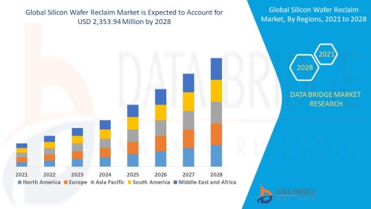
Silicon Wafer Reclaim Market Surge to Witness Huge Demand at a CAGR of 17.05% during the forecast period 2028
Industry Analysis
Silicon wafer reclaim market size is valued at USD 2,353.94 million by 2028 is expected to grow at a compound annual growth rate of 17.05% in the forecast period of 2021 to 2028. Data Bridge Market Research report on silicon wafer reclaim provides analysis and insights regarding the various factors expected to be prevalent throughout the forecasted period while providing their impacts on the market’s growth.
Additionally, the credible Silicon Wafer Reclaim Market report helps the manufacturer in finding out the effectiveness of the existing channels of distribution, advertising programs, or media, selling methods and the best way of distributing the goods to the eventual consumers. Taking up such market research report is all the time beneficial for any company whether it is a small scale or large scale, for marketing of products or services. It makes effortless for Semiconductors and Electronics industry to visualize what is already available in the market, what market anticipates, the competitive environment, and what should be done to surpass the competitor.
Get a Free Sample of The Report: https://www.databridgemarketresearch.com/request-a-sample/?dbmr=global-silicon-wafer-reclaim-market
Market Insights and Scope
Silicon wafer reclaim is a type of multi-step procedure which transforms a used wafer with numerous layers of various materials into a qualification wafer. The major steps integrated in wafer reclaim are sorting, stripping, lapping and grinding, polishing, cleaning and the inspection.
The Silicon Wafer Reclaim Market report encompasses various segments linked to Semiconductors and Electronics industry and market with comprehensive research and analysis. These comprise industry outlook with respect to critical success factors (CSFs), industry dynamics that mainly covers drivers and restraints, market segmentation & value chain analysis, key opportunities, application and technology outlook, regional or geographical insight, country-level analysis, key company profiles, competitive landscape, and company market share analysis. All the data, figures and information are backed up by well recognized analysis tools which include SWOT analysis and Porter’s Five Forces analysis. So, take business to the peak level of growth with the all-inclusive Data Bridge Market research report.
Get full access to the report: https://www.databridgemarketresearch.com/reports/global-silicon-wafer-reclaim-market
Industry Segmentation and Size
Silicon wafer reclaim market is segmented on the basis of reclaim capacity, application and end user. The growth among segments helps you analyze niche pockets of growth and strategies to approach the market and determine your core application areas and the difference in your target markets.
On the basis of reclaim capacity, the silicon wafer reclaim market is segmented into 150 mm, 200 mm, 300 mm and >300 mm.
The application segment of the silicon wafer reclaim market is segmented into integrated circuits, solar cells, photoelectric cells and others.
Based on end user, the silicon wafer reclaim market is segmented into automotive, aerospace and defense, mining and construction, electronics and others. Others have further been segmented into medical and sports.
Market Country Level Analysis
The countries covered in the silicon wafer reclaim market report are
U.S., Canada and Mexico in North America, Brazil, Argentina and Rest of South America as part of South America, Germany, Italy, U.K., France, Spain, Netherlands, Belgium, Switzerland, Turkey, Russia, Rest of Europe in Europe, Japan, China, India, South Korea, Australia, Singapore, Malaysia, Thailand, Indonesia, Philippines, Rest of Asia-Pacific (APAC) in the Asia-Pacific (APAC), Saudi Arabia, U.A.E, South Africa, Egypt, Israel, Rest of Middle East and Africa (MEA)as a part of Middle East and Africa (MEA).
A reliable Silicon Wafer Reclaim Market marketing report proves to be the finest and excellent market research report as it is formulated with the following critical factors. These consist of primary research, benchmarking studies, secondary research, company profiles, competitive intelligence & reporting, syndicated research, data collection, data processing and analysis, survey design, and survey programming. The report performs market study and analysis to provide market data by considering new product development from beginning to launch. The Semiconductors and Electronics business report also provides evaluations based on the market type, organization size, availability on-premises, end-users’ organization type, and the availability in areas such as North America, South America, Europe, Asia-Pacific and Middle East & Africa.
Industry Share Analysis
The major players covered in the silicon wafer reclaim market report are
NanoSILICON, Inc., AnySilicon, Pure Wafer, Silicon Valley Microelectronics, Inc., Noel Technologies, Inc., RS Technologies Co., Ltd., Phoenix Silicon International Corporation, Polishing Corporation of America, Naura-Akrion, Optim Wafer Services, KINIK COMPANY, Silicon Specialist LLC, Global Silicon Technologies, Nippon Chemi-Con Corporation, DSK Technologies Pte Ltd., and MicroSil, LLC among other domestic and global players. Market share data is available for global, North America, Europe, Asia-Pacific (APAC), Middle East and Africa (MEA) and South America separately.
Browse Related Reports@
Global Whiskey Market
South Africa Battery Market
Global Plant-Based Egg Market
Global Nutritional Beverages market
MENA Tahini market
Global Dental Membrane and Bone Graft Substitute Market
About Us:
Data Bridge Market Research set forth itself as an unconventional and neoteric Market research and consulting firm with an unparalleled level of resilience and integrated approaches. We are determined to unearth the best market opportunities and foster efficient information for your business to thrive in the market
Contact:
Data Bridge Market Research
Tel: +1-888-387-2818
Email: [email protected]
#Silicon Wafer Reclaim Market Growing Popularity#Silicon Wafer Reclaim Market Global Leading Brands#Silicon Wafer Reclaim Market drivers-advantages#Silicon Wafer Reclaim Market Segmentation-CAGR rate#Silicon Wafer Reclaim Market Demands-Size-Share-Top Trends#Silicon Wafer Reclaim Market Industry-Competitors#Silicon Wafer Reclaim Market Growth-Competition#Silicon Wafer Reclaim Market 2028 by Types-Application#Silicon Wafer Reclaim Market Semiconductors and Electronics Industry
0 notes
Link
In 2017, the International Trade Center (ITC) had measured that the global value of the semiconductor industry was $2.48 billion.[1]According to the Semiconductor Industry Association (SIA), global semiconductor sales had registered an upsurge on 12.7% year-to-year in October 2018, and the organization had projected 2.6% growth in 2018.[2] Silicon wafers are used in the manufacturing process of a gamut of semiconductor components, and the estimated escalation in the revenues generated in the semiconductor industry is having a positive influence on the silicon wafers market that offered opportunities worth $402.27 million as of 2018. Furthermore, the demand for silicon wafers is projected to observe a healthy compound annual growth rate (CAGR) of 8.50% during the forecast period of 2019 to 2025.
The automotive and consumer electronics sector is on the rise in APAC. This is largely attributed to economic growth in APAC countries that include China, India, Japan, Indonesia, and the Philippines, which is leading to a surge in demand for consumer electronic products such as mobile, television, digital cameras, and others. Furthermore, the soaring sales of automotive vehicles are evident in the fact that residents in the region are now able to afford motor cars and other vehicles which is creating a need for semiconductors. The demand for semiconductors in the region is leading to an augmented increase in revenues generated in the silicon wafers market. APAC had the maximum silicon wafers market share of 32.36% in 2018.
Silicon Wafers Market Outlook:
A silicon wafer is a semiconductor wafer which is used for the fabrication of integrated circuits and wafer-based solar cells. A unit wafer fabrication step such as etch step can produce more wafer chips to increase the area of overall silicon wafer. Owing to the indispensable application in semiconductors, the customer-base for the vendors in the silicon wafers market is found to be in consumer electronics, telecommunications, automotive, and healthcare industries.
Owing to the rapidly increasing number of mobile devices that has been well-documented by the Global System for Mobile Communication (GSMA. According to the organization, the total number of unique mobile subscribers in 2018 were gauged to be 5.1 billion, and the number is estimated to escalate at a moderate CAGR of 1.9% through to 2025.[3] This will have a direct impact on the consumer electronics application segment of the silicon wafers market, which is project to observe a superlative CAGR of 11.34% over the forecast period of 2019 to 2025.
Request Sample
Silicon Wafers Market Growth Drivers:
· The Growth Prospects in the Automotive Industry –
The International Organization of Motor Vehicle Manufacturers (OICA) has measured the total number of vehicles that were produced in 2018, and the figure translates to a striking 91.54 million.[4] The future foresees an increase production rate in the automotive industry in which the contribution from the autonomous vehicles, electric vehicles, and self-driving trucks will play a vital role. Resultantly, this augmentation in the production of vehicles will create a myriad of opportunities for the vendors in the silicon wafers market.
· The Increased Implementation of GPS Tracking System –
GPS tracking device market is booming as the system has penetrated into almost every industry. These devices create a major silicon wafers marketplace because semiconductors are an integral part of GPS systems. Furthermore, there is a continuous R&D in progress and the future innovations in the GPC tracking industry will further propel the silicon wafers market.
· The Application Segment in the Healthcare Sector Supporting the Market –
The augmented application of semiconductors in the healthcare sector can be fathomed by the growth prospects in the healthcare equipment market. Silicon wafers find application in the semiconductors that are incorporated in the healthcare equipment. The future is poised to observe surging sales of healthcare equipment which will further flourish the silicon wafers market.
Inquiry Before Buying
Silicon Wafers Market Trends –
· The Developments in Internet of Things –
The advances in the IoT will be creating a broad spectrum for semiconductors because they will be used in the devices that will be connected with each other through a mobile application. This will create a potential and sustainable silicon wafers marketplace.
· Latest Development –
In November 2017, Soitec which holds a significant market share in the silicon wafers market developed the latest generation of silicon-on-insulator (SOI) which will find applications in virtual reality (VR), augmented reality (AR), and 3D cameras.
Silicon Wafers Market Challenges –
The major challenge faced by the vendors in the silicon wafers market is the high initial investment with a questionable lack of returns. Furthermore, there are problems pertaining to handling and processing as they are thin and require external mechanical support, and more so when it comes to handling 450mm silicon wafers for semiconductor manufacturing. Thus, it becomes imperative to use specially designed chucks, rigid career wafers, and dicing tape which further shoots up the budget. On top of that, the final packaging is cumbersome. However, the market size for the silicon wafers is poised to observe an expansion which is the main reason vendors are ready to make investments in manufacturing. The future foresees more vendors venturing into the market because of the enhanced demand due to the technological advancements in AR, VR, IoT, and AI.
Buy Now
Silicon Wafers Market Key Players Perspective –
The major players striving to capitalize on the demand influx in the silicon wafers market are Elkem AS, Addison Engineering, Renewable Energy Corporation, Shin-Etsu Handotai Co. Ltd, Siltronic AG, MEMC Electronic Materials Inc, LG Siltron Inc, Advance Semiconductor Inc., and SUMCO Corp.
Silicon Wafers Market Research Scope:
The base year of the study is 2018, with forecast done up to 2025. The study presents a thorough analysis of the competitive landscape, taking into account the market shares of the leading companies. It also provides information on unit shipments. These provide the key market participants with the necessary business intelligence and help them understand the future of the silicon wafers market. The assessment includes the forecast, an overview of the competitive structure, the market shares of the competitors, as well as the market trends, market demands, market drivers, market challenges, and product analysis. The market drivers and restraints have been assessed to fathom their impact over the forecast period. This report further identifies the key opportunities for growth while also detailing the key challenges and possible threats. The silicon wafers market research report also analyses the application of silicon wafers in the consumer electronics, telecommunications, automotive, and healthcare industry.
Silicon Wafers Market Report: Industry Coverage
This report also documents the product demand on the basis of wafer size that include 150, 200, 300mm and doping material including N-Type & P-Type. The market is further segmented into epitaxial, diffused, and SOI.
The silicon wafers market report also analyzes the major geographic regions as well as the major countries in these regions. The regions and countries covered in the study include:
North America: The U.S., Canada, Mexico
South America: Brazil, Venezuela, Argentina, Ecuador, Peru, Colombia, Costa Rica
Europe: The U.K., Germany, Italy, France, the Netherlands, Belgium, Spain, Denmark
APAC: China, Japan, Australia, South Korea, India, Taiwan, Malaysia, Hong Kong
Middle East and Africa: Israel, South Africa, Saudi Arabia
For more Electronics related reports, please click here
0 notes
Text
Silicon Carbide Wafer Market 2022 to 2027 - Global Analysis By Type, By Applications
The report covers comprehensive data on emerging trends, market drivers, growth opportunities, and restraints that can change the market dynamics of the industry. It provides an in-depth analysis of the Silicon Carbide Wafer Market segments which include product types, applications, and competitor analysis. The report also includes a detailed study of key companies to provide insights into business strategies, company summary, trading summary, business strategy and planning, SWOT analysis and current developments adopted by various players in order to sustain competition in this highly competitive environment.
Silicon Carbide Wafer Market is envisaged to record an expansion at the CAGR of 7.8% over the forecast period, 2022 – 2027.
Read the full report:
The study objectives of this report are:
-An overview of the global market for Silicon Carbide Wafer Market and related technologies.
-Analyses of global market trends, with data, and projections of compound annual growth rates (CAGRs) through 2022-2027.
-Identifications of new market opportunities and targeted promotional plans for Global Silicon Carbide Wafer Market.
-Discussion of research and development, and the demand for new products and new applications.
#Silicon Carbide Wafer Market Opportunity#Silicon Carbide Wafer Market Size#Silicon Carbide Wafer Market Growth#Silicon Carbide Wafer Market Research
0 notes
Link
#Silicon Epitaxial Wafer Market Size Silicon Epitaxial Wafer Market Size#Silicon Epitaxial Wafer Market Price
0 notes
Text
Electronics engineers successfully integrate MoS₂ transistors on a 200 mm wafer
In recent years, electronics engineers have been trying to design increasingly sophisticated transistors that can be scaled down to smaller sizes. Given the limitations of conventional silicon-based field effect transistors (FETs), some teams have been experimenting with alternative designs based on materials with higher electron mobility.
Transition metal dichalcogenides (TMDs) are among the most promising materials for the development of scalable FETs, due to their small length and good carrier mobility. One of these materials is molybdenum disulfide (MoS2), a compound consisting of molybdenum and sulfide atoms in a 1:2 ratio.
Researchers at Samsung Advanced Institute of Technology (SAIT) and Seoul National University recently demonstrated integration of MoS2 transistors on a 200 mm wafer. Their paper, published in Nature Electronics, demonstrates the scalability of transistors based on MoS2, highlighting their potential for the future development of smaller and flexible devices.
Read more.
#Materials Science#Science#Transistors#Electronics#Transition metal dichalcogenides#Field effect transistors#Molybdenum disulfide#Molybdenum#Sulfides#2D materials
10 notes
·
View notes
Text
Chinese scientists have made a significant breakthrough in the world of semiconductors, the South China Morning Post (SCMP) reports. Just one atom thick (thereby termed "2D"), the new 12-long (30.5 cm) wafers can be cheaply and potentially revolutionize the semiconductor industry, its creators claim. While more work is needed to turn them into usable microchips, the new wafers could complement, even challenge, traditional silicon chips.
Due to its thinness, the new 2D material exhibits superior semiconducting properties. However, the team of scientists faced challenges when it came to scaling up the size of the wafers and producing them in large quantities. “We proved to the industry that this is scientifically feasible and instilled confidence. If there are industrial demands in the future, progress in this field will advance by leaps and bounds,” study lead Professor Liu Kaihui of Peking University told SCMP in an exclusive interview.
As reported in a study published in Science Bulletin, the new wafers offer some critical improvements over existing silicon chips. “When silicon transistors are made thinner, their [voltage control] becomes worse. Current will exist even when the device is not working. This brings extra energy costs and heat generation,” Liu explained.
The new 2D material comprises crystalline solids with one or several atom layers. Due to its naturally atomic-level thickness, the wafers possess unique physical properties and have potential applications in high-performance electronic devices. “A transistor built from a single layer of MoS2, [a typical 2D material] with a thickness of about one nanometre, outperforms the one made with the same thickness of silicon many times,” Liu added.
[...] to date, scientists have struggled to fabricate 2D material wafers with high uniformity and device performance, even though 2D materials can exist separately at each layer. The new wafers can be stacked layer by layer, including materials such as graphene or transition metal dichalcogenides (TMDs) like molybdenum disulfide, tungsten disulfide, molybdenum diselenide, and tungsten diselenide.
28 Aug 23
37 notes
·
View notes
Note
can you guys chill lmao. just trying to help
Sapphire is a precious gemstone, a variety of the mineral corundum, consisting of aluminium oxide (α-Al2O3) with trace amounts of elements such as iron, titanium, cobalt, lead, chromium, vanadium, magnesium, boron, and silicon. The name sapphire is derived from the Latin word sapphirus, itself from the Greek word sappheiros (σάπφειρος), which referred to lapis lazuli. It is typically blue, but natural "fancy" sapphires also occur in yellow, purple, orange, and green colors; "parti sapphires" show two or more colors. Red corundum stones also occur, but are called rubies rather than sapphires. Pink-colored corundum may be classified either as ruby or sapphire depending on locale. Commonly, natural sapphires are cut and polished into gemstones and worn in jewelry. They also may be created synthetically in laboratories for industrial or decorative purposes in large crystal boules. Because of the remarkable hardness of sapphires – 9 on the Mohs scale (the third hardest mineral, after diamond at 10 and moissanite at 9.5) – sapphires are also used in some non-ornamental applications, such as infrared optical components, high-durability windows, wristwatch crystals and movement bearings, and very thin electronic wafers, which are used as the insulating substrates of special-purpose solid-state electronics such as integrated circuits and GaN-based blue LEDs. Sapphire is the birthstone for September and the gem of the 45th anniversary. A sapphire jubilee occurs after 65 years.
Sapphire is one of the two gem-varieties of corundum, the other being ruby (defined as corundum in a shade of red). Although blue is the best-known sapphire color, they occur in other colors, including gray and black, and also can be colorless. A pinkish orange variety of sapphire is called padparadscha.
Significant sapphire deposits are found in Australia, Afghanistan, Cambodia, Cameroon, China (Shandong), Colombia, Ethiopia, India Jammu and Kashmir (Padder, Kishtwar), Kenya, Laos, Madagascar, Malawi, Mozambique, Myanmar (Burma), Nigeria, Rwanda, Sri Lanka, Tanzania, Thailand, United States (Montana) and Vietnam. Sapphire and rubies are often found in the same geographical settings, but they generally have different geological formations. For example, both ruby and sapphire are found in Myanmar's Mogok Stone Tract, but the rubies form in marble, while the sapphire forms in granitic pegmatites or corundum syenites.
Every sapphire mine produces a wide range of quality, and origin is not a guarantee of quality. For sapphire, Jammu and Kashmir receives the highest premium, although Burma, Sri Lanka, and Madagascar also produce large quantities of fine quality gems.
The cost of natural sapphires varies depending on their color, clarity, size, cut, and overall quality. Sapphires that are completely untreated are worth far more than those that have been treated. Geographical origin also has a major impact on price. For most gems of one carat or more, an independent report from a respected laboratory such as GIA, Lotus Gemology, or SSEF, is often required by buyers before they will make a purchase.
9 notes
·
View notes
Text
Semiconductor Market - Forecast (2022 - 2027)
Semiconductor market size is valued at $427.6 billion in 2020 and is expected to reach a value of $698.2 billion by 2026 at a CAGR of 5.9% during the forecast period 2021-2026. Increased investments in memory devices and Integrated circuit components are driving technological improvements in the semiconductor sector. The emergence of artificial intelligence, internet of things and machine learning technologies is expected to create a market for Insulators as this technology aid memory chip to process large data in less time. Moreover demand for faster and advanced memory chip in industrial application is expected to boost the semiconductor market size. Semiconductors technology continues to shrink in size and shapes, a single chip may hold more and more devices, indicating more capabilities per chip. As a result, a number of previously-used chips are now being combined into a single chip, resulting in highly-integrated solutions. Owing to such advancement in technology the Gallium arsenide market is expected to spur its semiconductor market share in the forecast period.
Report Coverage
The report: “Semiconductor Market Forecast (2021-2026)”, by IndustryARC covers an in-depth analysis of the following segments of the Semiconductor market report.
By Components – Analog IC, Sensors, MPU, MCU, Memory Devices, Lighting Devices, Discrete Power Devices, Others
By Application – Networking & Communication, Healthcare, Automotive, Consumer electronic, Data processing, Industrial, Smart Grid, Gaming, Other components
By Type - Intrinsic Semiconductor, Extrinsic Semiconductor
By Process- Water Production, Wafer Fabrication, Doping, Masking, Etching, Thermal Oxidation
By Geography - North America (U.S, Canada, Mexico), Europe (Germany, UK, France, Italy, Spain, Belgium, Russia and Others), APAC(China, Japan India, SK, Aus and Others), South America(Brazil, Argentina, and others), and RoW (Middle east and Africa)
Request Sample
Key Takeaways
In component segment Memory device is expected to drive the overall market growth owing to on-going technological advancement such as virtual reality and cloud computing.
networking and communication is expected hold the large share owing to rise in demand for smart phone and smart devices around the world.
APAC region is estimated to account for the largest share in the global market during the forecast period due to rise of electronic equipment production and presence of large local component manufacturers.
Semiconductor Market Segment Analysis- By Component
Memory device is expected to drive the overall market growth at a CAGR of 6.1% owing to on-going technological advancement such as virtual reality and cloud computing. High average selling price of NAND flash chips and DRAM would contribute significantly to revenue generation. Over the constant evolution, logic devices utilised in special purpose application particular signal processors and application specific integrated circuits are expected to grow at the fastest rate.
Inquiry Before Buying
Semiconductor Market Segment Analysis - By Application
With increasing demand for smart phone and smart devices around the world networking and communication segment is expected hold the large share in the market at 16.5% in 2020. Moreover due to Impact of Covid 19, the necessity of working from home has risen and the use of devices such as laptops, routers and other have increased which is expected to boost the semiconductor market size. The process of Wafer Level Packaging (WLP), in which an IC is packaged to produce a component that is nearly the same size as the die, has increased the use of semiconductor ICs across consumer electronics components owing to developments in silicon wafer materials.
Semiconductor Market Segment Analysis – By Geography
APAC region is estimated to account for the largest semiconductor market share at 44.8% during the forecast period owing to rise of electronic equipment production. Due to the extensive on-going migration of various electrical equipment and the existence of local component manufacturers, China is recognised as the region's leading country. The market in North America is expected to grow at a rapid pace, owing to rising R&D spending.
Schedule a Call
Semiconductor Market Drivers
Increase in Utilization of Consumer Electronics
Rise in technological advancement in consumer electronic devices have created a massive demand for integrated circuit chip, as these IC chip are used in most of the devices such as Smartphones, TV’s, refrigerator for advanced/ smart functioning. Moreover investment towards semiconductor industries by the leading consumer electronics companies such as Apple, Samsung and other is expected to boost the semiconductor market share by country. The adoption of cloud computing has pushed growth for server CPUs and storage which is ultimately expected to drive the semiconductor market. Wireless-internet are being adopted on a global scale and it require semiconductor equipment As a result, the semiconductor market research is fuelled by demand and income created by their production.
AI Application in Automotive
Semiconductor industry is expected to be driven by the huge and growing demand for powerful AI applications from automotive markets. Automakers are pushing forward with driverless vehicles, advanced driver assistance systems (ADAS), and graphics processing units (GPUs) which is estimated to boost the semiconductor market size. Furthermore, varied automobile products, such as navigation control, entertainment systems, and collision detection systems, utilise automotive semiconductor ICs with various capabilities. In the present time, automotive represents approximately 10 – 12 per cent of the chip market.
Buy Now
Semiconductor Market- Challenges
Changing Functionality of Chipsets
The semiconductor market is being held back by the constantly changing functionality of semiconductor chips and the unique demands of end-users from various industries. The factors such as Power efficiency, unrealistic schedules, and cost-down considerations are hindering the semiconductor market analysis.
Semiconductor Market Landscape
Technology launches, acquisitions and R&D activities are key strategies adopted by players in the Semiconductors Market. The market of Electrical conductivity has been consolidated by the major players – Qualcomm, Samsung Electronics, Toshiba Corporation, Micron Technology, Intel Corporation, Texas Instruments, Kyocera Corporation, Taiwan Semiconductor Manufacturing, NXP Semiconductors, Fujitsu Semiconductor Ltd.
Acquisitions/Technology Launches
In July 2020 Qualcomm introduced QCS410 AND QCS610 system on chips, this is designed for premium camera technology, including powerful artificial intelligence and machine learning features.
In November 2019 Samsung announced it production of its 12GB and 24GB LPDDR4X uMCP chip, offering high quality memory and data transfer rate upto 4266 Mbps in smartphones
In September 2019 the new 5655 Series electronic Board-to-Board connectors from Kyocera Corporation are optimised for high-speed data transfer, with a 0.5mm pitch and a stacking height of under 4mm, making them among the world's smallest for this class of connector.
For more Electronics related reports, please click here
3 notes
·
View notes
Text
Application of aluminum nitride in the semiconductor field
01 Substrate materials and packaging materials
With the vigorous development of microelectronics and semiconductor technology, current-power semiconductor devices need to have high voltage, high current, high power density, small size, and other characteristics at the same time. The heat flow density of electronic substrates has increased significantly, and maintaining a stable operating environment inside the equipment has become a focus. Technical issues of concern. For this reason, substrate materials in power-integrated circuits must have both good mechanical reliability and high thermal conductivity. At present, packaging substrate materials mainly use alumina ceramics or polymer materials. However, as the requirements for carrier substrates for electronic parts become more and more stringent, their thermal conductivity cannot meet the needs of the industry. AlN ceramics have thermal conductivity It has the characteristics of high thermal expansion coefficient, close to the thermal expansion coefficient of silicon, high mechanical strength, good chemical stability and environmental protection, and non-toxicity. It is considered to be an ideal material for the new generation of heat-dissipation substrates and electronic device packaging. Compared with the Al2O3 ceramic substrate and Si3N4 ceramic substrate, the AlN ceramic substrate has these advantages: using the AlN ceramic substrate as the carrier of the chip can isolate the chip from the module heat dissipation bottom plate, and the AlN ceramic layer in the middle of the substrate can effectively improve the insulation capability of the module. (Ceramic layer insulation withstands voltage >2.5KV), and the aluminum nitride ceramic substrate has good thermal conductivity, and the thermal conductivity can reach 170-260W/mK. In addition, the expansion coefficient of the AlN ceramic substrate is similar to that of silicon, which will not cause stress damage to the chip. The peeling resistance of the AlN ceramic substrate is >20N/mm2. It has excellent mechanical properties, and corrosion resistance, and is not prone to deformation. It can be used in a wide range of applications. Use within temperature range.
02 Electrostatic chuck for wafer processing
The wafer processing process in modern semiconductor manufacturing processes involves multiple processes. The wafers need to be transferred back and forth between hundreds of process equipment, so a device is needed to clamp the wafers. The electrostatic chuck can fix the wafer through electrostatic adsorption. The adsorption force is uniform and stable. The wafer will not warp and deform, ensuring the processing accuracy and cleanliness of the wafer. The current common electrostatic chuck technology mainly uses alumina ceramics or aluminum nitride ceramics as the main material. For ordinary silicon wafer processing, high-purity alumina or sapphire can meet the requirements. However, if used in silicon carbide wafer processing, the thermal conductivity is insufficient, and aluminum nitride must be used to meet the requirements.
The advantage of the aluminum nitride ceramic electrostatic chuck is that it can obtain a wide temperature range and sufficient adsorption force by controlling its volume resistivity. The electrostatic chuck can achieve good temperature uniformity through a heater design with a high degree of freedom; Nitrogen Aluminum is integrally co-fired and will not undergo changes over time due to electrode degradation, ensuring product quality to the greatest extent; it can operate for a long time in a plasma halogen vacuum atmosphere to withstand the most demanding process environments of semiconductors and microelectronics. It also provides stable adsorption and temperature control.
03 Substrate material
AlN crystal is an ideal substrate for GaN, AlGaN, and AlN epitaxial materials. Compared with sapphire or SiC substrates, AlN and GaN have higher thermal matching and chemical compatibility, and less stress between the substrate and the epitaxial layer. Therefore, when AlN crystal is used as a GaN epitaxial substrate, it can greatly reduce the defect density in the device, improve the performance of the device, and have good application prospects in the preparation of high-temperature, high-frequency, and high-power electronic devices. In addition, using AlN crystal as an AlGaN epitaxial material substrate with a high aluminum (Al) component can also effectively reduce the defect density in the nitride epitaxial layer and greatly improve the performance and service life of nitride semiconductor devices. High-quality solar blind detectors based on AlGaN have been successfully used.
04 Thin film materials
Due to AlN's wide band gap, strong polarization, and bandgap width of 6.2eV, the aluminum nitride thin film material prepared by it has many excellent physical and chemical properties, such as high breakdown field strength, high thermal conductivity, high resistivity, and high Due to its chemical and thermal stability, as well as good optical and mechanical properties, it is widely used as an isolation medium and insulating material in the packaging of electronic devices and integrated circuits. The high-quality AlN film also has the characteristics of extremely high ultrasonic transmission speed, small acoustic wave loss, considerable piezoelectric coupling constant, and thermal expansion coefficient similar to Si and GaAs. Its unique properties make it widely used in machinery, and microelectronics, There are broad application prospects in the fields of optical and electronic components, surface acoustic wave device manufacturing, and high-frequency broadband communications. At present, the preparation of aluminum nitride thin films is still at a stage where the equipment is complex, expensive, and difficult to commercialize, and the method used to prepare the thin films usually requires heating the substrate to a relatively high temperature. At present, the method of preparing aluminum nitride thin films at low temperatures is not mature and perfect. The development of integrated optical devices requires thin film preparation at lower temperatures to avoid thermal damage to the substrate material. There is still a lot of work to be done to improve the preparation method of aluminum nitride films and obtain denser, more uniform, higher purity, and lower-cost aluminum nitride films at lower temperatures and simpler process conditions.
0 notes
Text
0 notes
Text
Europe Silicon Carbide Wafers Market size, Scope, Growth Opportunities, Trends by Manufacturers and Forecast to 2029

Industry Analysis
Europe silicon carbide wafers market is expected to gain market growth in the forecast period of 2022 to 2029. Data Bridge Market Research analyses that the market is growing with a CAGR of 21.5% in the forecast period of 2022 to 2029 and is expected to reach USD 910,354.97 thousand by 2029.
Additionally, the credible Europe Silicon Carbide Wafers Market report helps the manufacturer in finding out the effectiveness of the existing channels of distribution, advertising programs, or media, selling methods and the best way of distributing the goods to the eventual consumers. Taking up such market research report is all the time beneficial for any company whether it is a small scale or large scale, for marketing of products or services. It makes effortless for Semiconductors and Electronics industry to visualize what is already available in the market, what market anticipates, the competitive environment, and what should be done to surpass the competitor.
Get a Free Sample of The Report: https://www.databridgemarketresearch.com/request-a-sample/?dbmr=europe-silicon-carbide-wafers-market
Market Insights and Scope
Silicon carbide wafers refer to the type of semiconductor that contains carbon and silicon, which operates at very high voltage and temperature. Silicon carbide wafers can be used in producing a strong as well as a very hard material. Silicon carbide wafers can be implemented in various sectors such as telecommunication, energy & power, automotive, renewable power generation, and in different other areas. They are basically considered due to higher maximum thermal conductive properties that have widened the area of application. Silicon carbide wafers are the devices that are considered being high-frequency power devices that are majorly applicable in wireless communications.
An international Europe Silicon Carbide Wafers Market research report examines competitive companies and manufacturers in the global market. Competitive analysis carried out in this market report puts forth the moves of the key players in the Semiconductors and Electronics industry such as new product launches, expansions, agreements, joint ventures, partnerships, and recent acquisitions. This market report puts light on various aspects of marketing research that range from important industry trends, market size, market share estimates, sales volume, emerging trends, product consumption, customer preferences, historic data along with future forecast and key player analysis. It studies market by product type, applications and growth factors.
Get full access to the report:https://www.databridgemarketresearch.com/reports/europe-silicon-carbide-wafers-market
Industry Segmentation
Europe silicon carbide wafers market is segmented into four notable segments based on wafer size, device, applications and industries.
On the basis of wafer size, the Europe silicon carbide wafers market is segmented into 2-inch, 4 inch, and 6-inch and above. In 2022, the 4-inch segment is expected to dominate the market as high-voltage and high-power devices such as diodes, power transistors, and high-power microwave devices are fabricated using this size of SiC wafers.
On the basis of device, the Europe silicon carbide wafers market is segmented into SiC discrete devices and SiC bare die. In 2022, SiC discrete devices segment is expected to dominate the market as SiC-based power devices have faster-switching speed, higher voltages, lower parasitic resistances, smaller size, less cooling required due to high-temperature capability.
On the basis of application, the Europe silicon carbide wafers market is segmented into power grid device, industrial motor drive, EV motor drive, RF device & cellular base station, solar energy, wind energy, flexible AC transmission systems, high-voltage, direct current, electronic combat system, lighting control, EV charging, power supply and inverter, flame detector, and others. In 2022, the power grid device segment is expected to dominate the market as there is an increase in the continuously changing demand in electricity distribution along with huge investments in the adoption of smart grids to offer flexible power supply.
On the basis of industry, the Europe silicon carbide wafers market is segmented into telecommunication, energy & power, renewable power generation, automotive, power electronics, defence, and others. In 2022, the telecommunication segment is expected to dominate the market as there are increasing investments in developing telecommunication infrastructure for entertainment, news, social connectivity, and e-commerce in the region.
Industry Share Analysis
Some of the major players operating in the report are silicon carbide wafers market are
WOLFSPEED, INC., II-VI Incorporated, SHOWA DENKO K.K., American Elements, Atecom Technology Co., Ltd, Entegris, Ferrotec Holdings Corporation, Fuji Electric Co., Ltd., Infineon Technologies AG, Microchip Technology Inc., Mitsubishi Electric Corporation, MTI Corporation, PI-KEM Limited. Renesas Electronics Corporation. Robert Bosch GmbH, ROHM CO., LTD., Semiconductor Components Industries, LLC. SEMIKRON, SiCrystal GmbH, SK siltron Co., Ltd. (A Subsidiary of SK HOLDINGS CO., LTD.). STMicroelectronics, Texas Instruments Incorporated, TOSHIBA ELECTRONIC DEVICES & STORAGE CORPORATION, and WeEn Semiconductors, among others. DBMR analysts understand competitive strengths and provide competitive analysis for each competitor separately.
Market Country Level Analysis
The countries covered in Europe silicon carbide wafers market report are the
U.K., Germany, France, Spain, Italy, Netherlands, Switzerland, Russia, Belgium, Turkey, Luxemburg, and the rest of Europe.
Germany is expected to dominate the market in the Europe region due to the increasing adoption of cost-effective energy storage methods and the rise in the application of silicon carbide wafers in the semiconductor industry.
An influential Europe Silicon Carbide Wafers Market research report displays an absolute outline of the market that considers various aspects such as product definition, customary vendor landscape, and market segmentation. Currently, businesses are relying on the diverse segments covered in the market research report to a great extent which gives them better insights to drive the business on the right track. The competitive analysis brings into light a clear insight about the market share analysis and actions of the key industry players. With this info, businesses can successfully make decisions about business strategies to accomplish maximum return on investment (ROI).
Browse Related Reports@
Global Frozen Vegetables Market
South Africa Battery Market
Global Plant-Based Egg Market
Global Nutritional Beverages market
Spain Fuel Cards Market for Commercial Fleet
Europe Fall Detection System Market
About Us:Data Bridge Market Research set forth itself as an unconventional and neoteric Market research and consulting firm with an unparalleled level of resilience and integrated approaches. We are determined to unearth the best market opportunities and foster efficient information for your business to thrive in the market
Contact:
Data Bridge Market Research
Tel: +1-888-387-2818
Email: [email protected]
#Europe Silicon Carbide Wafers Market Growing Popularity and Traffic#Europe Silicon Carbide Wafers Market Global Leading Brands and Businesses#Europe Silicon Carbide Wafers Market drivers-advantages-restraints and challenges#Europe Silicon Carbide Wafers Market Value-Segmentation-CAGR rate-Future Trends to 2029#Europe Silicon Carbide Wafers Market Demands-Size-Share-Top Trends#Europe Silicon Carbide Wafers Market Industry Insights-Country-Competitors Research#Europe Silicon Carbide Wafers Market Growth-Competition-Scenario-Outlook#Europe Silicon Carbide Wafers Market Global Opportunity Analysis#Europe Silicon Carbide Wafers Market 2029 by Product-Types-Procedure-Application-End User#Europe Silicon Carbide Wafers Market Semiconductors and Electronics Industry
0 notes
Text
Global Top 7 Companies Accounted for 29% of total SiC Wafer Processing Industry Chain market (QYResearch, 2021)
SiC single crystal wafers have excellent heat resistance and voltage resistance compared to silicon wafers that are widely used for semiconductors. SiC single crystal wafers can remarkably reduce energy loss during electric power control, significantly contributing to the reduction of energy use and environmental stress. They are highly expected as substrate materials for the next-generation.
According to the new market research report “Global SiC Wafer Processing Industry Chain Market Report 2023-2029”, published by QYResearch, the global SiC Wafer Processing Industry Chain market size is projected to reach USD 1.33 billion by 2029, at a CAGR of 8.7% during the forecast period.
Figure. Global SiC Wafer Processing Industry Chain Market Size (US$ Million), 2018-2029

Figure. Global SiC Wafer Processing Industry Chain Top 7 Players Ranking and Market Share (Ranking is based on the revenue of 2022, continually updated)

The global key manufacturers of SiC Wafer Processing Industry Chain include Wolfspeed, II-VI Advanced Materials, TankeBlue, SiCrystal, Materials Research Furnaces, etc. In 2021, the global top four players had a share approximately 29.0% in terms of revenue.
About QYResearch
QYResearch founded in California, USA in 2007.It is a leading global market research and consulting company. With over 16 years’ experience and professional research team in various cities over the world QY Research focuses on management consulting, database and seminar services, IPO consulting, industry chain research and customized research to help our clients in providing non-linear revenue model and make them successful. We are globally recognized for our expansive portfolio of services, good corporate citizenship, and our strong commitment to sustainability. Up to now, we have cooperated with more than 60,000 clients across five continents. Let’s work closely with you and build a bold and better future.
QYResearch is a world-renowned large-scale consulting company. The industry covers various high-tech industry chain market segments, spanning the semiconductor industry chain (semiconductor equipment and parts, semiconductor materials, ICs, Foundry, packaging and testing, discrete devices, sensors, optoelectronic devices), photovoltaic industry chain (equipment, cells, modules, auxiliary material brackets, inverters, power station terminals), new energy automobile industry chain (batteries and materials, auto parts, batteries, motors, electronic control, automotive semiconductors, etc.), communication industry chain (communication system equipment, terminal equipment, electronic components, RF front-end, optical modules, 4G/5G/6G, broadband, IoT, digital economy, AI), advanced materials industry Chain (metal materials, polymer materials, ceramic materials, nano materials, etc.), machinery manufacturing industry chain (CNC machine tools, construction machinery, electrical machinery, 3C automation, industrial robots, lasers, industrial control, drones), food, beverages and pharmaceuticals, medical equipment, agriculture, etc.
0 notes
Text
News Briefs May 30- Google, Meta Solar PPAs, LONGi
https://www.merchant-business.com/news-briefs-may-30-google-meta-solar-ppas-longi/?feed_id=8831&_unique_id=665b307d2a23d
News Briefs May 30- Google, Meta Solar PPAs, LONGi
Google Signs First Solar PPAs In Japan
Technology giant Alphabet, which owns Google, has signed its first solar PPAs in Japan.
The virtual power purchase agreements (PPAs) adding up to 60 MW have been signed with two Japanese companies. The larger firm, involved with 40 MW of the planned capacity is Clean Energy Connect (CEC), a partner of the Itochu Corporation. CEC will construct around 800 small-scale solar plants across multiple Japanese grids, generating 40MW ac of power, which CEC expects to commission by September 2026.
Meta Signs 204 MW Deal For Solar In US
Facebook owner Meta has signed an environmental asset purchase agreement (EAPA) with Pinegate renewables for a 204MW solar PV project in Temple, Texas. The deal is meant to power a Meta data centre located close to the Limewood Bell Solar project of Pinegate.
LONGi Launches Hi-MO X6 ‘Standardised Wafer’ Size Modules
Global solar manufacturing major LONGi has launched a new solar module, which it said exhibits the benefits of standardised module and wafer sizes in the solar industry.
The Hi-MO X6 Max series module will be built at LONGi’s Jiaxing facility in China exceeding 30GW of annual production by Q3 2024. LONGi said that the modules are designed to meet the needs of distributed PV customers and feature ‘TaiRay Inside’ and Hybrid Passivated Back Contact (HPBC) cell technologies, offering increased stability and efficiency
Featuring rectangular 72-cell silicon wafers, the wafers deployed in these modules are 182.2mm x 191.6mm M11 products.
Source link
News Briefs May 30- Google, Meta Solar PPAs, LONGi #News #Briefs #Google #Meta #Solar #PPAs #LONGi
Source link Google News
Source Link: https://www.saurenergy.com/solar-energy-news/news-briefs-may-30-google-meta-solar-ppas-longis-hi-mo-x6-modules
The post News Briefs May 30- Google, Meta Solar PPAs, LONGi appeared first on Merchant Business News.
Buy, Sell, Get Informed, Negotiate and Be Happy!
Global, GoogleNews
0 notes
Text
News Briefs May 30- Google, Meta Solar PPAs, LONGi - #Global #GoogleNews
https://www.merchant-business.com/news-briefs-may-30-google-meta-solar-ppas-longi/?feed_id=8830&_unique_id=665b307c23a7f
News Briefs May 30- Google, Meta Solar PPAs, LONGi
Google Signs First Solar PPAs In Japan
Technology giant Alphabet, which owns Google, has signed its first solar PPAs in Japan.
The virtual power purchase agreements (PPAs) adding up to 60 MW have been signed with two Japanese companies. The larger firm, involved with 40 MW of the planned capacity is Clean Energy Connect (CEC), a partner of the Itochu Corporation. CEC will construct around 800 small-scale solar plants across multiple Japanese grids, generating 40MW ac of power, which CEC expects to commission by September 2026.
Meta Signs 204 MW Deal For Solar In US
Facebook owner Meta has signed an environmental asset purchase agreement (EAPA) with Pinegate renewables for a 204MW solar PV project in Temple, Texas. The deal is meant to power a Meta data centre located close to the Limewood Bell Solar project of Pinegate.
LONGi Launches Hi-MO X6 ‘Standardised Wafer’ Size Modules
Global solar manufacturing major LONGi has launched a new solar module, which it said exhibits the benefits of standardised module and wafer sizes in the solar industry.
The Hi-MO X6 Max series module will be built at LONGi’s Jiaxing facility in China exceeding 30GW of annual production by Q3 2024. LONGi said that the modules are designed to meet the needs of distributed PV customers and feature ‘TaiRay Inside’ and Hybrid Passivated Back Contact (HPBC) cell technologies, offering increased stability and efficiency
Featuring rectangular 72-cell silicon wafers, the wafers deployed in these modules are 182.2mm x 191.6mm M11 products.
Source link
News Briefs May 30- Google, Meta Solar PPAs, LONGi #News #Briefs #Google #Meta #Solar #PPAs #LONGi
Source link Google News
Source Link: https://www.saurenergy.com/solar-energy-news/news-briefs-may-30-google-meta-solar-ppas-longis-hi-mo-x6-modules
The post News Briefs May 30- Google, Meta Solar PPAs, LONGi appeared first on Merchant Business News.
Buy, Sell, Get Informed, Negotiate and Be Happy!
Global, GoogleNews
BLOGGER - #Global #GoogleNews
0 notes
Text
News Briefs May 30- Google, Meta Solar PPAs, LONGi
https://www.merchant-business.com/news-briefs-may-30-google-meta-solar-ppas-longi/?feed_id=8829&_unique_id=665b307ae7ba4
News Briefs May 30- Google, Meta Solar PPAs, LONGi
Google Signs First Solar PPAs In Japan
Technology giant Alphabet, which owns Google, has signed its first solar PPAs in Japan.
The virtual power purchase agreements (PPAs) adding up to 60 MW have been signed with two Japanese companies. The larger firm, involved with 40 MW of the planned capacity is Clean Energy Connect (CEC), a partner of the Itochu Corporation. CEC will construct around 800 small-scale solar plants across multiple Japanese grids, generating 40MW ac of power, which CEC expects to commission by September 2026.
Meta Signs 204 MW Deal For Solar In US
Facebook owner Meta has signed an environmental asset purchase agreement (EAPA) with Pinegate renewables for a 204MW solar PV project in Temple, Texas. The deal is meant to power a Meta data centre located close to the Limewood Bell Solar project of Pinegate.
LONGi Launches Hi-MO X6 ‘Standardised Wafer’ Size Modules
Global solar manufacturing major LONGi has launched a new solar module, which it said exhibits the benefits of standardised module and wafer sizes in the solar industry.
The Hi-MO X6 Max series module will be built at LONGi’s Jiaxing facility in China exceeding 30GW of annual production by Q3 2024. LONGi said that the modules are designed to meet the needs of distributed PV customers and feature ‘TaiRay Inside’ and Hybrid Passivated Back Contact (HPBC) cell technologies, offering increased stability and efficiency
Featuring rectangular 72-cell silicon wafers, the wafers deployed in these modules are 182.2mm x 191.6mm M11 products.
Source link
News Briefs May 30- Google, Meta Solar PPAs, LONGi #News #Briefs #Google #Meta #Solar #PPAs #LONGi
Source link Google News
Source Link: https://www.saurenergy.com/solar-energy-news/news-briefs-may-30-google-meta-solar-ppas-longis-hi-mo-x6-modules
The post News Briefs May 30- Google, Meta Solar PPAs, LONGi appeared first on Merchant Business News.
Buy, Sell, Get Informed, Negotiate and Be Happy!
0 notes
Text
0 notes
Last Seen Blogs

deliriumuwu
🌷 chaphemer

seshika10
Arpeggio

danawilliams0
Dana Williams

skatekeys
a pleasant presence

ursxy
忠誠