#And with all this I have to worry about electromagnetic fields and impedance and interference because they’re real electrical signals and
Text
Five years of physics at university level and I still don’t understand electricity, electromagnetism and analog or digital sound recording or amplification
#I’m like okay so the human voice makes sound the usual way. Vibrations in the air. Get that. Get how it’s produced how it’s transmitted and#how it is heard by humans. Fine. Then you’re saying they speak into a microphone and those vibrations are converted into varying voltages#and that signal travels through a cable to a sound desk and then travels through another cable to the speakers#Where the voltage signal is converted back into a vibrating thing which is pushing the air and is making sound as we know it#And somehow after all that electricity we’ve now got a faithful reproduction of that human voice but louder now#And then you tell me. You do the first part. But then the signal is sent to a computer and is sampled at a very high rate and the voltages#are converted into 1s and 0s (which are actually also voltages but they’re just binary signals. Like a voltage of 0 or 5mv. That kind of th#And this highly sampled voltage signal which is now represented as 1s and 0s can be written onto a cd or played directly from a computer#And somehow we get that human voice back#I DONT UNDERSTAND IT#how is voltage a sound 😭#And then there’s also magnetic tapes and vinyl records. Which again I get but also it’s coming back to recreating those voltage signals.#Either by a needle moving up and down over spinning grooves#Or something with magnetic tape I don’t know how tapes are actually read#But electricity. I don’t get it.#And with all this I have to worry about electromagnetic fields and impedance and interference because they’re real electrical signals and#come with all the electromag physics of that!
4 notes
·
View notes
Text
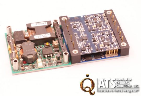
Industry Tips for Placing DC/DC Converters on PCB
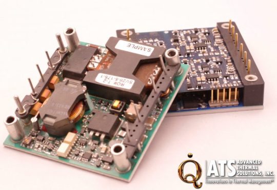
This article outlines industry tips and suggestions about placing DC/DC power converters on a PCB with other components. (Advanced Thermal Solutions, Inc.)
The design of a printed circuit board (PCB) that includes isolated DC to DC power converters is an important consideration to ensure the optimal performance of a system. Engineers have to be concerned with parasitic impedance and capacitance, the effects of the electromagnetic field created by the power converter on nearby components, as well as voltage accuracy, environmental noise reduction, and limiting radiated electro-magnetic interference (EMI).
This electromagnetic effect can cause significant voltage drops and improper design of a PCB could force engineers to make potentially costly changes (in terms of design time and budget), such as additional circuitry or upgrades to external components like power switches and capacitors.(i)
There are many advantages to using DC/DC converters and engineers adding these power bricks to a PCB do not have to be experts on power supply design, since the Distributed-power Open Systems Alliance (DOSA) has defined the industry standards for footprints and pinouts. Engineers know ahead of time how much space to dedicate and how the converter will be connected to the board.(ii)
“The brick typically comprises all the components (apart from filter circuits) required for a switching power supply including MOSFET switches, energy storage components, and switching controller,” writes Steven Keeping of Electronic Products on DigiKey.com. “By selecting a brick, an engineer does not have to worry about the intricacies of switching power supply design. The supplier has done all the work to ensure the unit operates optimally.”
While much of the work has been done by the manufacturer of the DC/DC converter to ensure its proper function, the engineer designing the system still has to consider the converter’s placement on a board carefully.
Parasitic Resistance, Impedance, and Capacitance
The most prominent issue that DC/DC converters can cause on a PCB is parasitic resistance, capacitance, and impedance. The power module creates an electromagnetic field that could disrupt the performance of components within its boundaries. As noted above, this could cause an unwanted voltage drop for the system and force more external power to be pushed through the converter.
According to a report published by members of the Institute of Electrical and Electronics Engineers (IEEE) from Georgia Tech University, “Short and wide routing traces have lower parasitic resistances and inductances and therefore superimpose less ill-fated effects to the system. As a result, to reduce the parasitic resistance and inductance, the first rule in PCB layout is to place connected power components as close as possible and in a way that their interconnection lengths are minimal.”(iii)
An article on DigiKey.com adds, “The signal traces should not be routed underneath the module, unless they are sandwiched between ground planes, to avoid noise coupling. Similarly, to prevent any coupling, no component should be placed under the module.”(iv)
The IEEE report continued, “Ground planes are effectively close high-speed return paths for average forward signal paths, but arbitrarily increasing the ground plane may not necessarily reach critical nodes. In PCB technologies with more than two layers, middle layers are normally dedicated to ground planes, thereby decreasing their distance to high-current forward switching paths.”
It also recommended using parallel connections for the supply ground, load ground, and measurement instrument’s ground rather than series connectors that are potentially unreliable and that can add impedance between nodes. The report stated, “Undesired noise and high temperature gradients across the PCB usually result when problems with supply ground connections exist.”
DC/DC converters regulate the voltage supply to the system from external power supplies, which makes accuracy a critical component of its performance. In order to ensure the optimal accuracy, it is recommended that the feedback sense terminal is connected as close to the load as possible. It is this voltage that will be converted.
(Advanced Thermal Solutions, Inc.)
Radiated Electromagnetic Interference
Another major concern for placing a DC/DC converter on a PCB is the amount of radiated electromagnetic interference (EMI) is emitted from the module. This is limited by industry standards (CISPR in Europe and FCC in the U.S.) but, as converters work by converting input voltage to AC before converting it back to DC at the correct voltage, there is an electromagnetic field that is produced when the converter is in use.
To minimize the effects of this EMI, “High-frequency nodes should be as short as possible. The metal paths act as antennas and their frequency range is directly proportional to their length. High frequency signal-return paths should be as close as possible to their respective forward paths. The two traces will therefore generate equal but opposite magnetic fields, canceling each other and hence reducing radiated EMI.”(v)
Tim Hegarty, writing for EDN Network, said, “A passive shield layer is established by placing a ground plane as close as possible to the switching loop by using a minimum dielectric thickness. The horizontal current flow on the top layer sets up a vertical flux pattern. The resulting magnetic field induces a current, opposite in direction to the power loop, in the shield layer.
“By Lenz’s Law, the current in the shield layer generates a magnetic field to counteract the original power loop’s magnetic field. The result is an H-field self-cancellation that amounts to lower parasitic inductance, reduced switch-node voltage overshoot, and enhanced suppression of EMI. Having an uninterrupted, continuous shield plane on layer 2 underneath and at closest proximity to the power loop offers the best performance.”(vi)
On DigiKey.com, Steve Taranovich of Electronic Products Magazine wrote, “The input of a DC/DC power module is a constant power at low frequencies. As the voltage decreases, current increases. This will present negative impedance at the input source. The converter will oscillate when the combination of the input filter’s impedance and the power module impedance becomes negative, causing a mismatch to occur. One way to prevent this is to ensure that the output impedance of the filter is much smaller than the input impedance of the power module at all frequencies.”(vii)
Another issue related to electromagnetic field is ground bounce, which is produced by changing magnetic flux due to the fast-changing currents. One of the solutions to prevent this problem, which could cause noise in video and audio devices, is to ensure that “true ground” is at the low end of the load and that all the other points are part of the ground return. In a two-layer PCB, Jeff Barrow of Analog.com also suggests, “A well-planned cut in the ground plane will constrain the return current to a minimum loop area and greatly reduce the bounce. Any residual bounce voltage that is developed in the cut return line is isolated from the general ground plane.”(viii)
Conclusions
Industry standard DC/DC converters have made adding a power supply to a PCB easier for engineers in terms of known sizes and connections. The footprint of a power module is known, but engineers still have important considerations to make before deciding where it should be placed. Keeping in mind the effects of parasitic impedance, capacitance, and resistance and ensuring that the electromagnetic interference will not surpass industry standards or affect other components on the board will ensure optimal performance of the system as a whole.
Using the design tips that are listed here, engineers are well on their way to creating an effective PCB layout with a DC/DC converter. Using Advanced Thermal Solutions, Inc. (ATS) Power Brick heat sinks will ensure the proper thermal management of the converters and of the board.
Learn more about Power Brick heat sinks at https://www.qats.com/eShop.aspx?productGroup=0&subGroup=2&q=Power%20Brick.
For more information about Advanced Thermal Solutions, Inc. thermal management consulting and design services, visit www.qats.com or contact ATS at 781.769.2800 or [email protected].
References
i http://rincon-mora.gatech.edu/research/pcb.pdf
ii http://www.digikey.com/en/articles/techzone/2012/dec/an-introduction-to-board-mounted-dcdc-converter-bricks
iii http://rincon-mora.gatech.edu/research/pcb.pdf
iv http://www.digikey.com/en/articles/techzone/2012/jul/proper-pcb-layout-minimizes-noise-coupling-for-point-of-load-converter-modules
v http://rincon-mora.gatech.edu/research/pcb.pdf
vi http://www.edn.com/design/power-management/4439749/3/DC-DC-converter-PCB-layout–Part-2
vii http://www.digikey.com/en/articles/techzone/2011/dec/conducted-and-radiated-emissions-reduction-techniques-for-power-modules
viii https://pdfs.semanticscholar.org/e3bb/49a1403b2da7d3d77e7024f7be208ee3a732.pdf
0 notes
Last Seen Blogs

angry-goat
Bahhhhh🐐

hfuejii
제목 없음

lucycrimefightr
Be Kind, Take No Nonsense

mid-blog
Moodly

fucker-anon
Fucker Anon