#Thick copper PCB
Text

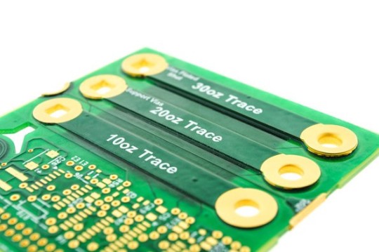
What is Heavy Copper PCB?
Heavy copper PCB is a circuit board with a copper thickness that is ≥ 3oz per sq. ft in its outer and inner layers. What makes a circuit board classified as a heavy copper PCB is its thicker plating. During the production of heavy copper PCB, copper thickness is enhanced through plated holes and sidewalls. For instance, when a PCB has 2 ounces of copper per sq. ft thickness, it is a standard PCB. However, if it has more than 3oz of copper, it is a heavy copper PCB. Heavy copper PCB is considered a reliable wiring option. Heavy copper PCB is different from extreme copper PCB which features within 20 oz to 200 oz per sq. ft.
What can Heavy Copper PCBs provide?
Heavy Copper PCBs have a lot to offer. It has some unique features that make it ideal for high-end applications. Let's discuss some of the benefits of this PCB;
• Great heat distribution: This PCB provides high thermal resistance due to its copper-plated through-hole. Heavy Copper PCBs are used in applications requiring high speed and high frequency. You can also use this PCB in harsh temperatures.
• Mechanical strength: Heavy Copper PCBs have very high mechanical strength. When used, this PCB makes the electrical system durable and rugged.
• Good conductor: Heavy Copper circuit boards are good conductors. Because of this property, they are used in the production of electronic products. They help hold the various plates together. These plates can transmit electricity.
• Onboard radiators: Heavy Copper PCB provide onboard radiators. Using these plates, you can achieve an effective radiator on a Mosaic surface.
• Large dissipation coefficient: Heavy Copper PCBs are ideal for large components with high power consumption. These PCBs prevent the electrical system from overheating. They dissipate heat effectively.
Hitech Circuits is a professional PCB manufacturer with extensive experience in manufacturing Heavy Copper PCBs, as well as your other product requirements. We support sample and mass production, welcome to your inquiry. Email [email protected] for a quick quote.
0 notes
Text
What is Heavy Copper PCB?
Heavy copper PCB is a circuit board with a copper thickness that is ≥ 3oz per sq. ft in its outer and inner layers. What makes a circuit board classified as a heavy copper PCB is its thicker plating. During the production of heavy copper PCB, copper thickness is enhanced through plated holes and sidewalls. For instance, when a PCB has 2 ounces of copper per sq. ft thickness, it is a standard PCB. However, if it has more than 3oz of copper, it is a heavy copper PCB. Heavy copper PCB is considered a reliable wiring option. Heavy copper PCB is different from extreme copper PCB which features within 20 oz to 200 oz per sq. ft.
What does Heavy Copper PCB offer?
Heavy copper PCB has a lot to offer. It has got some unique features that make it an ideal option for high-end applications. Let’s discuss some of the benefits of this PCB; Great thermal distribution: Due to its copper-plated vias, this PCB offers high thermal resistance. Heavy copper PCB are used in applications that demand high speed and high frequency. You can also use this PCB at harsh temperatures. Mechanical strength: Heavy copper PCB feature great mechanical strength. When this PCB is used, it makes the electrical system durable and robust. Good conductor: Heavy copper circuit boards are a good conductor. They are utilized in the production of electronics due to this feature. They help to link various boards together. These boards can transfer current.
How is Heavy Copper PCB Fabricated?
For the fabrication of heavy copper PCB, plating or etching is often used. The main aim is to add copper thickness to sidewalls and plated holes. The methods used in fabricating heavy copper PCB aren’t far-fetched. Heavy copper PCBs need special etching and plating methods to ensure the extra thickness of copper. Using the normal etching techniques for the fabrication of heavy copper PCBs isn’t ideal. Normal etching methods produce over-etched margins and edge lines that are uneven. PCB producers now use advanced etching and plating methods to achieve straight edges.
Heavy copper PCBs are produced via etching and plating methods. The major aim in the production of this PCB is to add copper thickness through sidewalls and plated-through holes. Heavy copper PCBs have several benefits which make them in high demand. Due to their outstanding features and benefits, they can meet your electrical requirements. These circuit boards will always dissipate heat generated due to heavy currents conduction. Electronics using heavy copper boards have been in use for a long time. Heavy copper can carry high currents. These boards will continue to meet the needs of various applications. High power circuit wirings can be developed using Heavy Copper PCBs. Such a wiring mechanism offers more reliable thermal stress handling and offers fine finishing while incorporating multiple channels on a single layer of a compact board.
Printed circuit boards (PCBs) are usually bonded with a layer of copper foil on a glass epoxy substrate. The thickness of the copper foil is usually 18μm, 35μm, 55μm, and 70μm. The most commonly used copper foil thickness is 35μm. Domestic copper foil thickness is generally 35 ~ 50μm, there are thinner than this such as 10μm, 18μm; And thicker than that like 70μm. The thickness of composite copper foil on 1~ 3mm thick substrate is about 35μm. The thickness of the composite copper foil on the substrate less than 1 mm thick is about 18μm, and the thickness of the cladding copper foil on the substrate thicker than 5mm is about 55μm. If the PCB copper foil thickness is 35μm, printed line width is 1mm, then every 10mm long, its resistance value is about 5mΩ, its inductance is about 4nH. When the di/dt of the digital integrated circuit chip on the PCB is 6mA/ns and the working current is 30mA, the noise voltage generated by each part of the circuit is estimated to be 0.15mV and 24mV according to the resistance value and inductance value of each 10mm printed line. Heavy Copper PCB boards can be made simply by combining two main processes: electroplating and etching. Compared to other PCBs, the circuit is made of a thin layer of copper foil. The copper plates are uniformly laminated with FR4 or other epoxy-based substances. The average weight of a Heavy Copper PCB can be 4 oz. (140μm), which is a better ratio than a copper-shared PCB. Let's look at the benefits.
Heavy Copper PCB Manufacturer & Circuit board Assembly – One-stop service Printed Circuit Boards (PCB) are usually coated with thick copper foil on a glass epoxy substrates commonly thickness of copper foil are 18μm, 35μm, 55μm, and 70μm. The most common copper foil is 35μm. The heavy copper PCB boards can simply be manufactured by two main processes plating and etching in the combine. As compared to other PCBs, the circuit is made of a thin layer of the Copper foil sheet. The plates of copper are laminated uniformly with FR4 or other epoxy-based substance. The average weight of the thick copper PCB weight could be 4oz (140μm), and this ratio is better as compared to another type of PCBs who have copper in common. Let’s check out the benefits of it.
Benefits of Heavy copper PCB Fabrication
Here are some of the advantages of heavy copper PCB, let’s follow them:
1. Favorable circumstances of Heavy Copper PCB
2. Plating innovation in overwhelming copper permitted a mix of plating and carving which causes in straight sidewalls and immaterial undercut.
3. The substantial copper plating creates high-current circuits and control circuits that watches the profoundly thick and straightforward whiskers’ structure.
4. This empowers the board fabricator to build the measure of copper thickness in plated gaps and by means of sidewalls.
5. The blend of substantial copper results on a solitary board called PowerLink.
6. The substantial copper in the PCB likewise encourages in associating with the standard circuits.
7. This lessens layer tally, low impedance control conveyance, littler impressions, and potential cost investment funds.
8. For development purposes, it expands the continuance to warm strains.
9. It has expanded the current conveying limit.
10. Overwhelming copper plating brings higher current through the board and moves the warmth to the outside heat sink
1 note
·
View note
Text
my custom keeb + sounds:
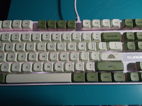
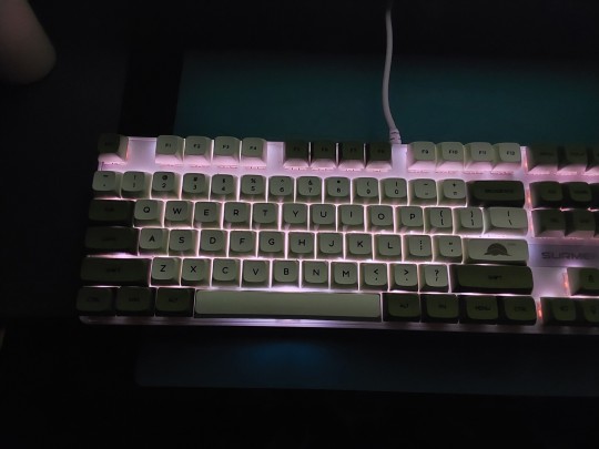

more info below, if u wanna see what i did
its around 65 CAD dollars on amazon, but i got it for 15 using a giftcard my old teacher gave me (i cleaned my highschools fish tanks for 3 years, wasnt expecting any payment but she gave me some money seeing as i would work 1-3 hours daily, sometimes all 5 days of the school week to keep those fish from dying, its a long story eurrr).
it came with the matcha keycaps + some extra keycaps for customization, rgb backlights, and some generic red linear switches (felt like 55g springs) which i later switched out for aliexpress fake holy pandas (67g springs), which are considered one of the best tactile switches out there, and the fake ones are honestly pretty close to the real ones. The stock red linears were good, especially for a starter enthusiast i think, but they were barely lubed and the springs inside were so LOUD. i thought the case was empty because of how loud the spring ping was LOL. to fix it, just l.ube the springs well.
they came factory lu.bed but i still went over them with my own aliexpress (again. i did not want to spend a lot of money) l.ube. they have crazy thock and when over-lub.ed, become creamy.
i did the foam mod using thick felt foam (also from ali.... it was precut to fit perfectly okay) plus another layer of that thin white packaging foam from the keyboard box. Unfortunately, the keyboard, despite saying it can be customized in its description, had the plate and the back case welded :/// i had to cut around the foam to slip it through the welded parts.
i added the thin white foam and some painters tape to the inside of the spacebar keycap to create more thock, which worked very well.
the new ali switches also didnt fit in the front plate?? they fit in the pcb just fine, but the front plate was a little too small or something so when i would push the switches in, theyd fly out. i had to put the thing on the floor and step on it to get some of the keys to stay. i eventually had to frankenstein the original red linear switch cases with the internals of the pandas to get the spacebar and enter keys to sit right and fit with the stabilizers.
the stabilizers are white plastic and removable, as long as you unsrew the entire top part of the case first LOL. they work fine with the stock switches, but struggle to move the keys up or down without sticking if you use any other switch.
the fekker holy pandas worked well, especially since they were fakes and a lot cheaper than the real ones - real pandas cost about 83 CAD for 70 pcs, while i got 110 for 25 CAD! there were a few in the bag that didnt work, and they were shipped in a plain plastic bag, but they give you extras so you have enough working ones for a full size keyboard (which has 104 keys).
i accidentally damaged the pcb copper wiring stuff by pushing in a switch without checking if the pins were aligned; the pins bent instead of going into the holes and scratched the wires. because of this, i lost function in both the f11 function key and the print screen key. i dont ever use those so im fine with it.
long post over. i love her so much
3 notes
·
View notes
Text
PCB Via Current-Carrying Capacity: Is My PCB Too Hot?

In the realm of printed circuit board (PCB) design, one of the critical factors that significantly impact the performance and reliability of a circuit is the current-carrying capacity of vias. Vias are the small plated-through holes that interconnect different layers of a PCB, facilitating the flow of electrical signals and power. However, when subjected to excessive current loads, vias can generate significant heat, leading to thermal issues and potential PCB failure.
Understanding the current-carrying capacity of vias is crucial for ensuring proper thermal management in your PCB design. In this article, we will delve into the factors that affect via current-carrying capacity, explore thermal management strategies, and provide practical tips to help you determine if your PCB is running too hot.
Understanding Via Current-Carrying Capacity
The current-carrying capacity of a via is determined by several factors, including its physical dimensions, the materials used in its construction, and the thermal environment in which it operates. When current flows through a via, it encounters resistance, resulting in the generation of heat. The amount of heat generated is directly proportional to the current flowing through the via and its resistance.
1. Via Dimensions
The physical dimensions of a via, such as its diameter and length (thickness of the PCB), play a crucial role in determining its current-carrying capacity. Generally, larger diameter vias have lower resistance and can carry higher currents without overheating. Similarly, shorter vias have lower resistance and can dissipate heat more effectively than longer vias.
2. PCB Materials
The materials used in the construction of the PCB can also affect the current-carrying capacity of vias. Different materials have varying thermal conductivity properties, which influence their ability to dissipate heat. PCBs made of materials with high thermal conductivity, such as aluminum or copper, can effectively dissipate heat generated by vias, allowing them to carry higher currents.
3. Thermal Environment
The thermal environment in which the PCB operates plays a significant role in determining the current-carrying capacity of vias. Factors such as ambient temperature, airflow, and the presence of heat sinks or cooling systems can greatly impact the ability of vias to dissipate heat effectively.
Calculating Via Current-Carrying Capacity
Several methods and guidelines exist for calculating the current-carrying capacity of vias. One widely used approach is the IPC-2221 standard, which provides equations and tables to estimate the current rating of vias based on their dimensions and the materials used.
The IPC-2221 standard considers factors such as via diameter, plating thickness, copper weight, and the thermal resistance of the PCB materials. It provides equations to calculate the maximum current that can flow through a via without exceeding a specified temperature rise.
Another method for estimating via current-carrying capacity is through thermal simulation and analysis. Computer-aided design (CAD) tools and finite element analysis (FEA) software can be used to model the thermal behavior of vias under various current loads and environmental conditions. These simulations can provide valuable insights into the thermal performance of your PCB design and help identify potential hotspots or areas of concern.
Thermal Management Strategies for Vias
If your PCB design involves high current loads or operates in a thermally challenging environment, implementing effective thermal management strategies is crucial. Here are some approaches to consider:
1. Via Array Design
Instead of relying on a single large via to carry high currents, designers often opt for via arrays or multiple smaller vias in parallel. By distributing the current across multiple vias, the heat generation is reduced, and the overall current-carrying capacity is increased.
2. Thermal Vias
Thermal vias, also known as heat vias or thermal relief patterns, are strategically placed vias that act as thermal conductors, helping to dissipate heat from hot components or areas of the PCB. These vias are typically connected to larger copper areas or heat sinks, providing an efficient path for heat transfer.
3. Thermal Planes
Incorporating thermal planes, or solid copper planes, into your PCB design can significantly improve heat dissipation. These planes act as heat spreaders, distributing the heat generated by components and vias over a larger area, reducing hotspots and improving thermal management.
4. Thermal Interface Materials
When working with high-power components or dense via arrays, the use of thermal interface materials (TIMs) can be beneficial. TIMs, such as thermal pads or thermal greases, improve the thermal coupling between the PCB and heat sinks or cooling systems, enhancing heat transfer and dissipation.
5. Active Cooling Solutions
In extreme cases or applications with very high current loads, active cooling solutions like fans or liquid cooling systems may be necessary to maintain acceptable operating temperatures for vias and other components.
Signs of Overheating in PCBs
Even with careful design and thermal management strategies, overheating issues can still occur in PCBs. It is essential to be aware of the signs that indicate your PCB may be running too hot, allowing you to take corrective actions before failures occur. Some common indicators of overheating include:
Physical Damage: Discoloration, warping, or delamination of the PCB can be signs of excessive heat exposure.
Component Failure: Premature failure of components, such as capacitors or integrated circuits, may be caused by overheating.
Intermittent Operation: Circuits experiencing intermittent operation or glitches could be a result of thermal stress on components or vias.
Thermal Imaging: Using thermal imaging cameras or sensors can provide a visual representation of hotspots on your PCB, allowing you to identify areas of concern.
FAQs (Frequently Asked Questions)
How can I determine the current rating of a via in my PCB design? You can determine the current rating of a via by using the IPC-2221 standard equations or guidelines provided by the PCB manufacturer. These equations take into account factors such as via diameter, plating thickness, copper weight, and the thermal resistance of the PCB materials. Alternatively, you can perform thermal simulations or finite element analysis to estimate the current-carrying capacity based on your specific design and environmental conditions.
What are some common causes of via overheating? Common causes of via overheating include inadequate via dimensions (small diameter or excessive length), high current loads, poor PCB material selection (low thermal conductivity), lack of proper thermal management strategies, and harsh operating environments (high ambient temperatures or limited airflow).
Can via arrays help mitigate overheating issues? Yes, using via arrays or multiple smaller vias in parallel can significantly improve the current-carrying capacity and reduce heat generation. By distributing the current across multiple vias, the heat generation is reduced, and the overall thermal performance is enhanced.
How can thermal vias or thermal planes help with PCB thermal management? Thermal vias, also known as heat vias or thermal relief patterns, provide efficient paths for heat transfer from hot components or areas of the PCB to larger copper areas or heat sinks. Thermal planes, or solid copper planes, act as heat spreaders, distributing the heat generated by components and vias over a larger area, reducing hotspots and improving thermal management.
When should I consider active cooling solutions for my PCB design? Active cooling solutions, such as fans or liquid cooling systems, may be necessary in extreme cases or applications with very high current loads or power densities. If passive cooling methods (e.g., heat sinks, thermal vias, and thermal planes) are insufficient to maintain acceptable operating temperatures, active cooling solutions should be considered to ensure reliable and safe operation of your PCB.
Conclusion
Proper thermal management and via current-carrying capacity considerations are crucial for ensuring the reliable operation and longevity of your PCB designs. By understanding the factors that affect via current-carrying capacity, implementing effective thermal management strategies, and monitoring for signs of overheating, you can mitigate the risk of thermal issues and create robust and high-performing PCB designs.
The most cost-effective PCB manufacturer from China
2 notes
·
View notes
Text

Heavy Copper PCB
Heavy copper pcb manufacturering up to 26 OZ
Hitech is a professional heavy copper pcb, thick copper pcb board manufacturer, PCB power supplier from China, we have been associated with heavy copper pcb plating since 2000 and we have won good reputation in this industry. If you have customized heavy copper pcb needs, please don’t heisitate to conatct [email protected] .
Demand for heavy copper PCB in Electric automotive, Power charge, voltage transformer, Charging station, industrial controls, and military is growing very fast. More than 80% of the existing printed wiring board manufacturing is limited or not capable of producing reliable heavy copper printed circuit boards.
Hitech thick copper board technology offers the possibility to implement complex switches in limited space in combination with circuitry for high current levels. Multi-layer PCB has reliable processes to produce copper layer thicknesses up to 26 Oz .
Hitech heavy copper PCB normally used for high power rectifiers, Power charge, Transformaer, Charging station, computer, military, electric vehicle charging, power grid switching system, etc

What is heavy copper PCB board
Heavy copper PCB boards ( also being called thick copper board, power board etc ) are usually bonded with a layer of copper foil on a glass epoxy substrate. The thickness of copper foil is usually 18μm, 35μm, 55μm and 70μm. The most commonly used copper foil thickness is 35μm. The thickness of copper foil used in China is generally 35-50μm, and there are also thinner ones such as 10μm and 18μm; and thicker ones such as 70μm. The thickness of the composite copper foil on a substrate with a thickness of 1-3mm is about 35μm; the thickness of the composite copper foil on a substrate with a thickness of less than 1mm is about 18μm, and the thickness of a composite copper foil on a substrate with a thickness of more than 5mm is about 55μm. If the thickness of the copper foil on the PCB is 35μm and the printed line width is 1mm, then for every 10mm length, its resistance value is about 5mΩ, and its inductance is about 4nH. When the di/dt of the digital integrated circuit chip on the PCB is 6mA/ns and the working current is 30mA, the resistance and inductance contained in each 10mm printed line are used to estimate the noise voltage generated by each part of the circuit to be 0.15. mV and 24mV.

Advantages of heavy copper PCB board
Heavy copper plate has the characteristics of carrying large current, reducing thermal strain, and good heat dissipation.
1. The heavy copper circuit board can carry large current
In the case of a certain line width, increasing the copper thickness is equivalent to increasing the cross-sectional area of the circuit, which can carry a larger current, so it has the characteristic of carrying a large current.
2. Heavy copper circuit boards reduce thermal strain
Copper foil has a small electrical conductivity (also called electrical resistivity ), the temperature rise is small when a large current is passed, so it can reduce the amount of heat and thereby reduce the thermal strain.
Metal “conductors” are divided into: ” silver→copper→gold→aluminum→tungsten→nickel→iron ” according to conductivity.
3. The heavy copper circuit board has good heat dissipation
Copper foil has high thermal conductivity (thermal conductivity 401W/mK), which can play an important role in improving heat dissipation performance, so it has good heat dissipation;
Thermal conductivity refers to the heat transfer through an area of 1 square meter within 1H for a 1 meter thick material with a temperature difference of 1°C on both sides under stable heat transfer conditions, measured by W/m·K.
Heavy copper plate has the characteristics of carrying large current, reducing thermal strain, and good heat dissipation.
Disadvantages of heavy copper PCB board
The outer copper-clad plane must be separated by the surface components and signal lines. If there is a poorly grounded copper foil (especially the thin and long copper), it will become an antenna and cause EMI problems.
If the pins of electronic components are fully connected with copper, it will cause the heat to dissipate too fast, and it will be difficult to desolder and rework soldering. The copper-clad plane of the outer layer must be well grounded, and more vias need to be punched to connect to the main ground plane. If more vias are punched, it will inevitably affect the wiring channels, unless buried blind vias are used.

Applications of heavy copper PCB board
The application field and demand for thick copper plates have been rapidly expanded in recent years, and it has become a “hot” PCB variety with good market development prospects.
The vast majority of heavy copper PCBs are high-current substrates (current x voltage = power). The main application areas of high-current PCBs are two major areas: power modules and automotive electronic components. Some of its main terminal electronic product fields are the same as conventional PCBs (such as portable electronic products, network products, base station equipment, etc.), and some are different from conventional PCB fields, such as automobiles, industrial controls, and power modules.
High-current PCBs are different from conventional PCBs in terms of efficacy. The main function of a conventional PCB is to form a wire for transmitting information. The high-current PCB has a large current through it, and the main function of the substrate carrying the power device is to protect the current carrying capacity and stabilize the power supply. The development trend of such high-current PCB is to carry larger currents, and the heat emitted by larger devices needs to be dissipated. Therefore, the large currents passing through them are getting larger and larger, and the thickness of all the copper foils of the PCBs is getting thicker and thicker. The 6 oz copper thickness of the high-current PCBs manufactured now has become normal;
The application areas of heavy copper circuit boards include: mobile phones, microwaves, aerospace, satellite communications, network base stations, hybrid integrated circuits, power supply high-power circuits and other high-tech fields.
#heavy copper pcb#pcb#pcb assembly#pcb designer#pcb layout#pcb manufacturing#pcb production#pcb supplier
4 notes
·
View notes
Text
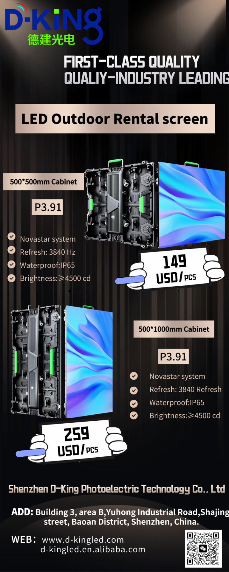
LED rental display, factory direct sales, price concessions.
→Model: P2.604/P2.976/P3.91/P4.81.
→ Module size: 250250mm. → Cabinet size: 500500mm/500*1000mm.
→ Lamp: SMD1415/SMD1921 copper lamp.
→PCB: 1.6mm thick flame retardant 4 layers
circuit board.
→ Receiving card: Novastar system.
→ Refresh: 3840 Refresh
→ Power supply: 5V 40A 200W.
………………………
WhatsApp: +86 18819048581
3 notes
·
View notes
Text
gnaws on pcb I ordered from a boardhouse one billion layers thick of copper foil epoxy and real bones press that shit NOW
2 notes
·
View notes
Text
Multi-purpose Skin And Also Hair Products For Women
Tidy hair roots will certainly lead to the hair expanding in the ideal direction. The skilled groomer must purchase a cleaning gadget-- especially if you have a beard of stubble. Our men's editor, Kirill Kutalov, is something of a males's grooming expert, so we assembled one of the most common men's skin and also hair treatment inquiries to get his professional recommendations obagi. " Normally sourced components, cedar and also cinammon crucial oils ... feels like a ruptured of freshness from the Himalayan wild." Anthocyanin, which increases blood circulation in the scalp, reinforcing hair follicles. It is taken into consideration among nature's most reliable ingredient for advertising hair development and also darkening hair normally.
The letters "FR" in the classification show Fire Resistance.
They may state that no excellent story ever started with a salad, but also for your total health and wellness as well as your skin it's extremely vital to mind your alcohol intake.
If you have sensitive skin, try a fragrance-free hair shampoo or conditioner.
Start your routine with our Coconut Exfoliating Lotion Body Scrub, a gentle rub-a-dub-dub helping to buff away any type of dead skin cells that could be spending time on the skin's surface.
Anthocyanin, which boosts blood circulation in the scalp, enhancing hair follicles.
PCB created for usage in vacuum or in zero gravity, as in spacecraft, being incapable to depend on convection cooling, frequently have thick copper or light weight aluminum cores to dissipate warmth from electric parts. Low-end consumer quality PCB substrates often are made from paper impregnated with phenolic resin, often branded "Pertinax". The product is low-cost, easy to machine by drilling shiseido , shearing as well as cold punching, as well as triggers less device wear than glass fiber reinforced substratums. The letters "FR" in the designation show Flame Resistance. The silk-screen, solder mask, as well as solder paste stencil are frequently created as supporting layers. Once transmitted, the system might have a series of technique subroutines to minimize the manufacturing expense of the PCB.
Brand
Body
2 notes
·
View notes
Text
0 notes
Text

Generally, rigid flex PCBs are used across various industries in applications for which a combination of flexibility, space efficiency, and high reliability is required. Rigid flex PCBs are often seen in aerospace and defense applications, like aircraft instrumentation and military equipment, as well as in the medical industry, where they are utilized in devices like implants and diagnostic equipment. Automotive electronics, industrial machinery and many other applications that demand an adaptable circuitry solution will also use rigid flex PCBs to great effect.
On a more granular level, rigid flex circuit boards are ideal for applications that present challenges to the circuitry during installation or operation. Flex-to-install applications, in which the circuit is designed to be flexed or bent during the installation process, call for rigid flex PCBs due to the application’s space constraints and/or the need for conformability to irregular shapes. In dynamic flex applications, the circuit will be continuously flexed during operation, so they are specifically designed to withstand and accommodate the ongoing mechanical stress without compromising their electrical performance or reliability. Rigid flex PCBs that follow the manufacturer’s recommended minimum bend radius offer hundreds of thousands of flex cycles without failure.
Applications in high-vibration environments present their own challenges that rigid flex PCBs overcome. Vibration generates mechanical stress that can impact circuits, causing them to flex and bend repeatedly during operation. This dynamic flexing can raise various concerns, including material fatigue, interconnect reliability issues, and component integrity failures.
To mitigate these risks, rigid flex PCBs designed for high-vibration environments are subjected to specific design and manufacturing considerations, like reinforcement to enhance their rigidity and mechanical stability or selecting a material with high flexural strength for their construction.
Finally, rigid flex PCBs are also commonly used in applications that handle high currents and generate heat, like high-speed data communication, industrial equipment or power electronics. Rigid flex PCBs generally have a higher current carrying capacity than rigid boards with flex circuit connections, which makes them a compelling choice for these applications — but that higher capacity comes at a cost.
In a phenomenon known as thermal expansion, the heat generated by a high current passing through a conductive trace or copper plane on a PCB causes the circuit material to expand and contract repeatedly. The flexible sections may undergo stretching or elongation, while the rigid sections experience minimal expansion; when the current stops or decreases, the PCB cools down and contracts. This presents several potential problems for the integrity of the circuit board, including the risks of mechanical stress and fatigue, as well as the risk of electrical performance issues.
But as with rigid flex PCBs designed for high-vibration applications, flex circuit board manufacturers can implement certain design and manufacturing considerations to help mitigate these risks. Choosing materials with good thermal stability and low coefficient of thermal expansion (CTE), implementing thermal management techniques like heat sinks and thermal vias, and optimizing the trace widths, thickness, and copper plane configurations can all help ensure the reliability and long-term performance of rigid flex PCBs in high-heat environments.
0 notes
Text

Ceramic PCB Manufacturing--Hitechpcba
Ceramic PCB board is also called ceramic substrate or ceramic circuit board, ceramic copper coated plate, ceramic substrate refers to the copper foil directly bonded to alumina (Al2O3) or aluminum nitride (AlN) ceramic substrate or other ceramic substrate surface (single or double) on the special process board. The ultrathin composite substrate has excellent electrical insulation performance, high thermal conductivity, excellent soft brazing and high adhesion strength, and can be etched into a variety of graphics like PCB board, with great current-carrying capacity. Therefore, Ceramic PCB board has become the basic material of high power electronic circuit structure technology and interconnection technology.
Ceramic PCB Manufacturing & Assembly – One-stop service The ceramic substrate (ceramic PCB) refers to a special process board in which a copper foil is directly bonded to a surface of an alumina (Al2O3 ) or aluminum nitride (AlN) ceramic substrate (single or double-sided) at a high temperature. The ultra-thin composite substrate produced has excellent electrical insulation properties, high thermal conductivity, excellent solderability, and high adhesion strength, and can etch various patterns like a PCB board, and has a large current carrying current ability.
The advantages and disadvantages of Ceramic PCB
(1) Ceramic PCB board has very good thermal conductivity and insulation performance. Ceramic PCB board is made of ceramic substrate, ceramic substrate itself has very good insulation and thermal conductivity, thermal conductivity of 25~230w, insulation resistivity is 10 minus 14 square, visible insulation performance is very good.
(2) The dielectric constant of ceramic PCB board is very low, the dielectric loss is small, has very good high frequency performance, the dielectric loss of alumina ceramic PCB board is less than 0.0003@1MHz, the dielectric loss of aluminum nitride ceramic PCB board is less than 0.0005@1MHz. Low dielectric loss, high frequency performance, is widely used in the field of high frequency communication.
(3) Ceramic PCB bonding force is strong, using bonding technology, copper foil will not fall off.
(4) Ceramic PCB has large on-board flow, 100A current continuously passes through 1mm0.3mm thick copper body, and the temperature rises about 17℃; when 100A current continuously passes through the 2mm0.3mm thick copper body, the temperature rises only about 5℃.
(5) Ceramic PCB board is with high temperature resistance, corrosion resistance, environmental protection, can work in a very complex environment, long-term high frequency, long service life.
Disadvantages: fragile, scrap rate is high, this is one of the main short comings of ceramic PCB board, which leads to the production of a small area of the circuit board, the general size is less than 120mm, special custom 200mm,230mm, the general price is more expensive, the board cost is higher. In addition, because ceramic PCB board is made of ceramic material, it does not have better toughness like FR4 board, so it can make more than one meter long and wide. Another point is that the price is expensive, the requirements of electronic products are more and more rules, ceramic circuit boards are still used in some relatively high-end products, low-end products will not be used.
With over 15 years of experience in the electronic industry we are committed to producing custom ceramic PCBs that meet up with the various electronic devices at hand.
0 notes
Text
What is Heavy Copper PCB or Thick Copper PCB?
In high-power applications, managing ultra-high thermal loads and high-power currents is crucial. Standard PCBs typically have copper thicknesses ranging from 1oz to 3oz. However, in scenarios requiring robust current management and thermal dissipation, Heavy Copper PCBs, also known as Thick Copper PCBs, come into play. These boards have finished copper weights between 4oz and 10oz, with some super thick copper PCBs reaching 20oz to 200oz per square foot. The increased copper thickness enables these PCBs to handle high current outputs and optimize thermal management, crucial for electronics applications where temperature control is paramount to avoid performance degradation and premature failure.
Additionally, thick copper layers allow for large PCB cross-sections, which are ideal for high current loads, and facilitate heat dissipation. These PCBs also enable the integration of finely laid out structures on the outer layers with thick copper layers on the inner layers, providing a versatile solution for various design requirements.
Construction of Heavy Copper PCB
Manufacturing thick copper PCBs involves a combination of etching and electroplating processes, similar to standard PCBs. However, special techniques are required to ensure that trace sidewalls and undercuts meet the standards for thick copper features. Some of the main challenges in manufacturing thick copper PCBs include the need to remove a significant amount of copper during etching, increased etching costs, and the difficulty in manufacturing thin traces and ensuring the evenness of thick traces.
How to Make Thick Copper PCB?
The manufacturing process for thick copper PCBs involves several key steps to ensure the even thickness of the copper layers. These steps include etching inner layer traces on each layer of the inner core material, designing pads with uniform spacing and positioning, and using appropriate methods for burying copper in the prepreg. Common processes for thick copper PCBs include inserting thick copper bars into the circuit board, using laminate deposition with a thick base copper, and burying copper in the prepreg using laser cutting.
Advantages of Heavy Copper PCBs
Heavy Copper PCBs offer several advantages over standard PCBs:
Excellent high heat resistance: Heavy Copper PCBs can withstand high temperatures, making them ideal for high-power applications.
Improved current carrying capacity: The increased copper thickness allows Heavy Copper PCBs to carry larger currents with the same line width.
Reduced complex wiring: Heavy Copper PCBs can simplify complex wiring configurations, leading to more efficient designs.
Compression of board size: Heavy Copper PCBs allow for the integration of multiple copper weights on the same PCB, reducing the overall size of the end-use product.
Enhanced mechanical strength: The use of thick copper in PCBs improves the mechanical strength of the board, particularly in areas such as PCB connector areas and plated through holes (PTH).
Improved thermal management: Heavy Copper PCBs facilitate better heat dissipation, which is crucial for maintaining the performance and longevity of electronic components.
Ordinary PCB vs. Heavy Copper PCB
The main differences between standard PCBs and Heavy Copper PCBs lie in the manufacturing process and the copper weight. Standard PCBs are made through processes such as etching, hole drilling, and electroplating, while Heavy Copper PCBs require finer differential pair etching and step plating processes to ensure trace quality. Additionally, the copper content per square foot of a standard PCB is between 1oz and 3oz, whereas for Heavy Copper PCBs, the copper content exceeds 3oz.
Difference between Copper PCB and Heavy Copper PCB
Copper PCBs and Heavy Copper PCBs serve different purposes, with the main distinction being the thickness of the copper foil. Copper PCBs refer to PCBs with a copper substrate, which helps dissipate heat and prolong the life of components. On the other hand, Heavy Copper PCBs have a copper thickness exceeding 3oz and are used for their high current-carrying capacity.
Characteristics of Heavy Copper PCBs
Heavy Copper PCBs offer several unique features:
Ultra-high mechanical strength: Thick copper layers enhance the mechanical strength of the PCB, making it more resistant to weather and external stresses.
Excellent weather resistance: Heavy Copper PCBs can withstand extreme temperatures and harsh environmental conditions, ensuring the stability of the circuit transmission signal.
Thermal management: Thick copper layers improve heat dissipation, crucial for modern, high-density PCBs with high current loads.
Excellent current conduction: Heavy Copper PCBs provide excellent conductivity, facilitating the transmission of electricity between various components.
Diversity: Heavy Copper PCBs support various conductive and substrate materials, production processes, and application fields, making them versatile for different design requirements.
In conclusion, Heavy Copper PCBs play a crucial role in high-power applications where robust current management and thermal dissipation are essential. Their unique construction and characteristics make them ideal for applications requiring high heat resistance, excellent current carrying capacity, and improved thermal management.
High quality PCB manufacturer from China
0 notes
Text
What is Heavy Copper PCB or Thick Copper PCB?
In high-power applications, managing ultra-high thermal loads and high-power currents is crucial. Standard PCBs typically have copper thicknesses ranging from 1oz to 3oz. However, in scenarios requiring robust current management and thermal dissipation, Heavy Copper PCBs, also known as Thick Copper PCBs, come into play. These boards have finished copper weights between 4oz and 10oz, with some super thick copper PCBs reaching 20oz to 200oz per square foot. The increased copper thickness enables these PCBs to handle high current outputs and optimize thermal management, crucial for electronics applications where temperature control is paramount to avoid performance degradation and premature failure.
Additionally, thick copper layers allow for large PCB cross-sections, which are ideal for high current loads, and facilitate heat dissipation. These PCBs also enable the integration of finely laid out structures on the outer layers with thick copper layers on the inner layers, providing a versatile solution for various design requirements.
Construction of Heavy Copper PCB
Manufacturing thick copper PCBs involves a combination of etching and electroplating processes, similar to standard PCBs. However, special techniques are required to ensure that trace sidewalls and undercuts meet the standards for thick copper features. Some of the main challenges in manufacturing thick copper PCBs include the need to remove a significant amount of copper during etching, increased etching costs, and the difficulty in manufacturing thin traces and ensuring the evenness of thick traces.
How to Make Thick Copper PCB?
The manufacturing process for thick copper PCBs involves several key steps to ensure the even thickness of the copper layers. These steps include etching inner layer traces on each layer of the inner core material, designing pads with uniform spacing and positioning, and using appropriate methods for burying copper in the prepreg. Common processes for thick copper PCBs include inserting thick copper bars into the circuit board, using laminate deposition with a thick base copper, and burying copper in the prepreg using laser cutting.
Advantages of Heavy Copper PCBs
Heavy Copper PCBs offer several advantages over standard PCBs:
Excellent high heat resistance: Heavy Copper PCBs can withstand high temperatures, making them ideal for high-power applications.
Improved current carrying capacity: The increased copper thickness allows Heavy Copper PCBs to carry larger currents with the same line width.
Reduced complex wiring: Heavy Copper PCBs can simplify complex wiring configurations, leading to more efficient designs.
Compression of board size: Heavy Copper PCBs allow for the integration of multiple copper weights on the same PCB, reducing the overall size of the end-use product.
Enhanced mechanical strength: The use of thick copper in PCBs improves the mechanical strength of the board, particularly in areas such as PCB connector areas and plated through holes (PTH).
Improved thermal management: Heavy Copper PCBs facilitate better heat dissipation, which is crucial for maintaining the performance and longevity of electronic components.
Ordinary PCB vs. Heavy Copper PCB
The main differences between standard PCBs and Heavy Copper PCBs lie in the manufacturing process and the copper weight. Standard PCBs are made through processes such as etching, hole drilling, and electroplating, while Heavy Copper PCBs require finer differential pair etching and step plating processes to ensure trace quality. Additionally, the copper content per square foot of a standard PCB is between 1oz and 3oz, whereas for Heavy Copper PCBs, the copper content exceeds 3oz.
Difference between Copper PCB and Heavy Copper PCB
Copper PCBs and Heavy Copper PCBs serve different purposes, with the main distinction being the thickness of the copper foil. Copper PCBs refer to PCBs with a copper substrate, which helps dissipate heat and prolong the life of components. On the other hand, Heavy Copper PCBs have a copper thickness exceeding 3oz and are used for their high current-carrying capacity.
Characteristics of Heavy Copper PCBs
Heavy Copper PCBs offer several unique features:
Ultra-high mechanical strength: Thick copper layers enhance the mechanical strength of the PCB, making it more resistant to weather and external stresses.
Excellent weather resistance: Heavy Copper PCBs can withstand extreme temperatures and harsh environmental conditions, ensuring the stability of the circuit transmission signal.
Thermal management: Thick copper layers improve heat dissipation, crucial for modern, high-density PCBs with high current loads.
Excellent current conduction: Heavy Copper PCBs provide excellent conductivity, facilitating the transmission of electricity between various components.
Diversity: Heavy Copper PCBs support various conductive and substrate materials, production processes, and application fields, making them versatile for different design requirements.
In conclusion, Heavy Copper PCBs play a crucial role in high-power applications where robust current management and thermal dissipation are essential. Their unique construction and characteristics make them ideal for applications requiring high heat resistance, excellent current carrying capacity, and improved thermal management.
2 notes
·
View notes
Text
Ceramic PCB manufacturing(from Hitech Circuits Co., Limited)
Ceramic PCB have good High thermal conductivity, ceramic substrate and conductor performance, excellent chemical and thermal stability. Excellent corrosion resistance, it widely used in semiconductor,Sensor and microelectronic circuit packaging pcb, High-brightness Led chip carrier board, automotive electronics and lighting components, high-power electronic component heat dissipation materials, etc.
Why Purchase Your Ceramic PCBs from HITECH CIRCUITS?
At HITECH CIRCUITS, we are dedicated to producing and selling quality PCBs to all of our customers. With over 15 years of experience in the electronic industry we are committed to producing custom ceramic PCBs that meet up with the various electronic devices at hand.
Our professionals manufacture nothing but top-notch ceramic PCBs that are developed to tackle your demands. In addition, we assure that you will get nothing but the best and affordable prices for all the quality ceramic PCB we manufacture. Regardless of the quality of the printed circuit boards that you want, it will be gotten at a decent price.
Ceramic PCB Parameter
Ceramic PCB in high pressure, high insulation, high frequency, high temperature, and high reliable and minor volume electronic products, then Ceramic PCB will be your best choice.
Why Ceramic PCB has such excellent performance?
96% or 98% Alumina (Al2O3), Aluminum Nitride (ALN), or Beryllium Oxide (BeO)
Conductors material: For thin film technology, thick film technology, it’ll be silver palladium (AgPd), gold pllladium (AuPd); For DCB (Direct Copper Bonded) it’ll be copper only
Application temp: -55~850C
Thermal conductivity value: 16W~28W/m-K (Al2O3); 150W~240W/m-K for ALN , 220~250W/m-K for BeO;
Max compression strength: >7,000 N/cm2
Breakdown Voltage (KV/mm): 15/20/28 for 0.25mm/0.63mm/1.0mm respectively
Thermal expansion conefficient(ppm/K): 7.4 (under 50~200C)
Contact Us
You can submit a custom request and get a price quote.
[email protected], from Cynthia.
1 note
·
View note
Video
flickr
Heavy copper PCB manufacturing by PCB Assembly
Via Flickr:
Heavy copper PCB is a circuit board with a copper thickness that is ≥ 3oz per sq. ft in its outer and inner layers. What makes a circuit board classified as a heavy copper PCB is its thicker plating. During the production of heavy copper PCB, copper thickness is enhanced through plated holes and sidewalls. For instance, when a PCB has 2 ounces of copper per sq. ft thickness, it is a standard PCB. However, if it has more than 3oz of copper, it is a heavy copper PCB. Heavy copper PCB is considered a reliable wiring option. Heavy copper PCB is different from extreme copper PCB which features within 20 oz to 200 oz per sq. ft. www.hitechpcba.com/heavy-copper-pcb-manufacturing
0 notes
Text

Increasing the thickness of the PCB sheet or strengthening the support structure around the large copper bar can help reduce warping deformation.
0 notes
Last Seen Blogs

shimlaandmanalitour
Shimla and Manali Tour

abeszelodiszno
a beszélő disznó

dokidobe
yellow.dr.monv

elaibee
aesthetic

justwantabigbootybitch97
I Need Help