
wslsolar
Custom Solar Panel - WSL Solar
WSL Solar has been a quality and professional manufacturer of customized solar panels and solar solution provider in China since 2006.
16 posts
Don't wanna be here? Send us removal request.
Last Seen Blogs

brookehameshair
Brooke Hames Hair

toshirocosplays
Toshiro Cosplays

vetometo
welcome to my scribbling corner

ury-omu
2020

phormlessblob
cupid stunt
Text
#custom solar panel#iot solar panel#small solar panel#tempered glass solar panel#solar panel for wireless sensors#WSL Solar
1 note
·
View note
Text
WSL Solar has been a professional manufacturer of high quality custom solar panels and solar solution provider in China since 2006.
If you are looking for custom solar panels for your solar application, please feel free to contact us. :-)
Email: [email protected]
https://www.wsl-solar.com
1 note
·
View note
Text
1 note
·
View note
Link
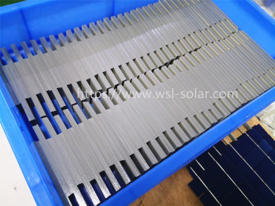
The construction of custom solar panels varies slightly depending on the lamination method and the materials used. The following is a brief introduction to the construction of tempered glass solar panels and ETFE solar panels.
1. Solar Panel Construction of Tempered Glass Solar Panels
Tempered Glass / EVA / Solar Cell / EVA / Backsheet
2. Solar Panel Construction of ETFE Solar Panels
ETFE film / EVA / Solar Cell / PCB
Tempered glass:
The role of tempered glass is to protect the solar cells, the selected photovoltaic glass must have high light transmittance (generally more than 91%), and requires ultra-white tempering treatment. The thickness of photovoltaic glass is either 3.2mm or 2.0mm. The most commonly used is the 3.2mm thick glass.
EVA:
EVA is an important encapsulant material, which is used to bond tempered glass and solar cells. It is usually cut into a thin sheet that can be inserted at the front and rear of the solar cells. The quality of transparent EVA material directly affects the lifespan of the solar panel. Should EVA be exposed to the air, it will easily age and turn yellow, thus affecting the light transmittance of the solar panel, and power generation quality.
The thickness of EVA ranges from 3mm to 4.5mm; among them, 4mm and 4.5mm are used the most.
Solar Cell:
Solar cells convert sunlight into electricity via the photovoltaic effect. They are the core parts of solar panels. Generally speaking, the power of a solar panel is proportional to the area of the solar cell.
Backsheet
The function of the backsheet is to seal, insulate and waterproof. Therefore, the selected backsheet materials such as TPT and TPE must be resistant to aging.
The backsheet is available in white and black. The white backsheet is commonly used, but some clients choose to use the black backsheet in order to maintain the color consistency with the application product and to be aesthetically pleasing.
ETFE Film:
ETFE film is a film used to protect solar cells inside solar panels. Its thickness is usually less than 0.2mm, making it thin and light. In addition, it has the characteristics of resistance to temperature changes, high light transmittance of up to 95%, high self-cleaning, corrosion resistance, and long service life.
IBC Solar Cell
ETFE solar panels adopt IBC solar cells (interdigitated back contact) with efficiency up to 24%, to achieve a higher power output in a limited area. Traditional solar cells achieve energy conversion by having front contacts in the cell, while IBC solar cells have the contacts on the rear side, instead of placing them in the front of the cell. This allows them to achieve higher efficiency due to reduced shading on the front of the cell, and also increases the aesthetics since no contacts are visible on the front. IBC solar cell technology also improves the temperature coefficient, which means an IBC solar panel can deliver a better performance in hot climate installations. It also has excellent performance under low light conditions.
WSL Solar has been a quality and professional manufacturer of custom solar panels, solar mini panels, IoT solar panels and solar solution provider in China since 2006.
https://www.wsl-solar.com
1 note
·
View note
Link
1 note
·
View note
Link
Silicon wafers are divided into semiconductor wafers and photovoltaic wafers according to their uses. Photovoltaic silicon wafers can be single crystal silicon or polycrystalline silicon, and semiconductor silicon wafers can only be single crystal silicon. The biggest difference between the two is that the content and purity of silicon are different. The conversion efficiency of monocrystalline silicon is generally about 18.5%~25%, and the conversion efficiency of polycrystalline silicon wafer is about 17.3%. Correspondingly, monocrystalline silicon solar cells have higher photoelectric conversion efficiency than polycrystalline silicon solar cells.
Over the years, the silicon wafer size has experienced a process from small to large. The increase in silicon wafer size and the continuous progress of photovoltaic technology have promoted the cost reduction and efficiency improvement of the entire photovoltaic industry chain.
For silicon wafer manufacturers, the larger size of silicon wafers can reduce the three major costs of silicon wafer companies: silicon material, crystal pulling, and slicing. The same amount of silicon material can reduce the number of crystal pulling and energy consumption when the diameter of the silicon rod becomes larger, thereby reducing the cost of crystal pulling. At the same time, large-sized silicon wafers can reduce the number of slices, the cost of slices and the cost per watt of silicon wafers.
For solar cell and solar panel manufacturers, the larger size of silicon wafers can speed up the production speed of silicon wafers to solar modules, which will also reduce production and operation costs such as manpower, water and electricity, and dilute the production process of solar cell modules. Non-silicon cost. As the size of a single silicon wafer increases, the number of cells in a single solar module decreases, the number of silicon wafers decreases accordingly, and the effective light-emitting area of the solar module increases, which will lead to an increase in conversion efficiency and power, and a decrease in the cost per watt. .
For power station customers, under the same power station scale, the larger the size of the solar modules, the less the number of solar modules required, thereby reducing the corresponding brackets, combiner boxes, cable costs, transportation and installation costs, etc. At the same time, large-sized silicon wafers will improve the power and quality of solar modules to a certain extent, and increase the power generation capacity of the power station while reducing the cost of the power station.
Under the driving force of diluting costs and improving the quality of solar modules, the silicon wafer size has grown from 100mm to 210mm in the past 40 years from 1981 to the present.
1981-2012: 100mm-156mm
Between 1981 and 2012, silicon wafers had margins of 100mm and 125mm, and were dominated by 125mm silicon wafers. After that, the margin of silicon wafer was greatly increased from 125mm to 156mm (ie M0), an increase of 54.1%. 156mm silicon wafer has gradually become a popular choice for p-type monocrystalline and polycrystalline silicon wafers. Around 2014, 125mm P-type silicon wafers were basically eliminated and only used in some IBC and HIT battery modules.
2012-2018: M0-M2
At the end of 2013, several major manufacturers took the lead in unifying M1 (margin 156.75mm, diameter 205mm) and M2 (margin 156.75mm, diameter 210mm) silicon wafers with a standard of 156.75mm, which is a major change in the history of silicon wafer size development. . In 2017, the size standard was reviewed and approved by the SEMI standards committee. The revised version of the national standard for polysilicon wafers in 2018 also determined 156.75mm as the standard side length, and suggested that future size increases should be changed in multiples of 1mm.
2018 to present: M2—M6
Under the situation of increasing demand for high-power components, some manufacturers began to achieve this goal by increasing the area of the battery, resulting in the emergence of 157.0, 157.3, 157.5, 157.75, 158.0 and other silicon wafers in the market. The organization and management of the chain brings great inconvenience.
After the melee, two mainstream sizes appeared on the market: G1 square monocrystalline (158.75mm margin) and M6 (166mm margin) large silicon wafers.
The ultimate in wafer size: 210mm
In August 2019, Zhonghuan launched the G12 (210mm margin) large silicon wafer, which greatly increased the area of the M6 silicon wafer by 60.8%. According to the data, the cost of G12 cells is 25.56% lower than that of M2, and the cost of components is reduced by 16.8%.
The change in the size of silicon wafers over the past 40 years reflects the parity process of the entire industry. With the advent of the parity era, a new starting point for the photovoltaic industry has just begun.
WSL Solar has been a quality and professional manufacturer of custom shape solar panels and solar solution provider in China since 2006.
https://www.wsl-solar.com
1 note
·
View note
Link
An exclusive opinion from the CEO of WSL Solar on how to choose the most suitable small solar panel for your system. Our CEO has more than 16 years of experience in the solar industry.
#small solar panel#mono perc solar panel#custom shaped solar panel#custom solar#WSL Solar#solar panels
1 note
·
View note
Link
0 notes
Link
Features:
- WSL Solar's 3V 10W solar panel adopts the latest PERC monocrystalline solar cell, >21% efficiency.
- Dimension 345x190x18mm
- Laminated by tempered glass, durable & robust
- Ideal for use in solar powered LED lighting, IoT solar,solar traffic sign and small solar powered systems etc.
#custom solar panel#10w solar panel#3v solar panel#WSL Solar#solar panel manufacturer#small solar panel
0 notes
Video
youtube
Different types of custom solar panels
Posted by Carrie Wong | WSL Solar Co., Ltd.
WSL Solar has been a quality and professional manufacturer of custom solar panels and solar solution provider in China since 2006.
https://www.wsl-solar.com
1 note
·
View note
Link
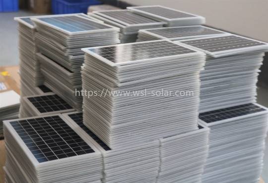
There are different types of custom solar panels: tempered glass solar panel or PET solar panel; mono solar panel or poly solar panel; black solar panel or white solar panel; with frame or not; with junction box or with ribbon only; need wire and terminal or not etc.
Do you know how to inquire a custom solar panel?
Hope this video could be helpful for you.
Posted by Carrie Wong | WSL Solar Co., Ltd.
WSL Solar has been a quality and professional manufacturer of customized solar panels and solar solution provider in China since 2006.
https://www.wsl-solar.com
1 note
·
View note
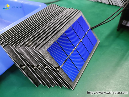
Link
IBC solar panels are built with the super high efficiency IBC solar cells (“Interdigitated back contact” solar cells). They are laminated by ETFE or PET film, which is light weight and thin. Thess customized solar panels are ideal for use in off grid applications such as IoT devices, smart phones, radio, Bluetooth, wireless sensors, RF Radio Sensitivity or solar gifts etc.
#IBC solar panel#IBC solar cell#custom solar panel#ETFE solar panel#PET solar panel#WSL Solar#small solar panel#IoT solar
1 note
·
View note
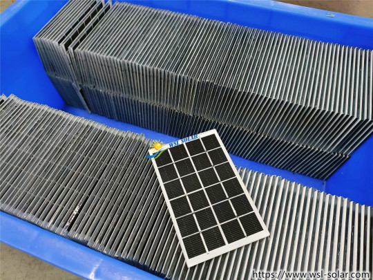
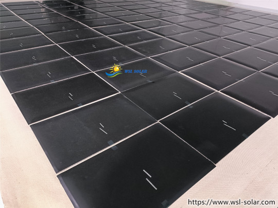
Photo

Quality Customized Solar Panel from WSL Solar.
Quality is always the first thing for us. We stick to strict quality control, from raw material sourcing, manufacturing process to finished product testing, we pay attention to details in each step, to deliver our clients the right solar panel for their solar application.
https://www.wsl-solar.com
#custom solar panel#WSL Solar#customized solar panel#small solar panel#solar panel#pv panel#solar energy panel
1 note
·
View note
Link
Posted by Carrie Wong | WSL Solar
WSL Solar has been a quality and professional manufacturer of custom solar panel and solar solution provider in China since 2006.
https://www.wsl-solar.com
1 note
·
View note
Link
Posted by Carrie Wong | WSL Solar
WSL Solar has been a quality and professional manufacturer of custom solar panel and solar solution provider in China since 2006.
https://www.wsl-solar.com
1 note
·
View note
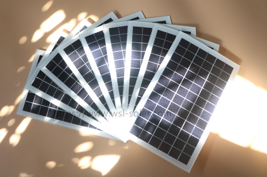
Photo

WSL Solar has been a quality and professional manufacturer of customized solar panels and solar solution provider in China since 2006.
https://www.wsl-solar.com
2 notes
·
View notes