#mc68030
Text
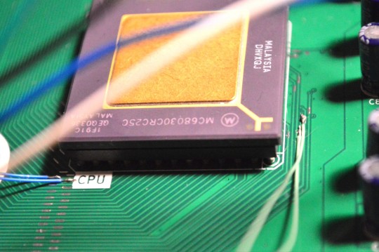
Revisiting Wrap030 Disk Access
I have more ideas for projects than time or budget to work on them. Already this year I've gone completely through the design process for two new large homebrew projects that are currently too large for my project budget, plus a few small ones I never got around to ordering. So rather than spend more than I should taking on a new project, I decided to revisit an existing one.
It's been over a year since I last worked on the original Wrap030 project — my old stack-of-boards MC68030 system. Its current configuration includes the main board with CPU, ROM, RAM, UART, & glue logic; a hand-wired breakout board to add a second UART; a custom video output board; and a mezzanine board with FPU and provision for an IDE disk that is not yet working. It has been functional in this configuration since last February.
My goal for this project from the beginning was to build something capable of running a proper operating system, like Unix System V or Linux. To do that though, I'm going to need to get disk access working.
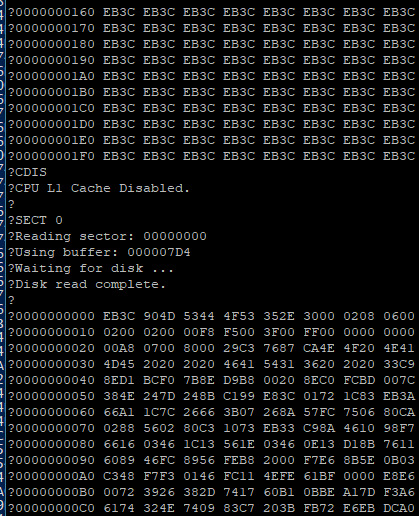
I had started on disk access, but didn't quite have it functional when I turned my focus to integrating all of boards into the single Wrap030-ATX motherboard. I had added IDE cycles to the CPLD on the mezzanine board, and had added a few rough drafts of disk functions to my ROM. I set the project aside when I realized my function for checking dish presence was reporting a disk was present when there wasn't one.
I have worked with IDE before — my original 68000 project had an IDE port on it. I had gotten that project to the point where I could read a sector of data from the disk, but never could wrap my head around how to actually navigate even a simple file system like FAT16. It was this code that I had adapted for Wrap030, so when it didn't work, I assumed it was a problem with my logic.
Turns out I had just inadvertently clobbered a register in the disk check function. The logic worked just fine. I was able to write a couple quick BASIC programs to read a sector of data and even run code from the boot sector.

My assembly function for reading data from disk however was still not working.
I tried rewriting it.
I tried rewriting it in C instead of assembly.
I tried again, and again, and again. I added delays and loops and print statements and everything I could think of. I scoured datasheets, read though all the different release versions of the ATA specification, ported code from other projects, looked at every example of reading from an IDE disk I could find.
No matter what I did, I always got the same result.
This did not make any sense. Reading from an IDE disk involves setting up the sector address, the number of sectors to transfer, sending a read command, and then reading the IDE data port 256 times per sector. Each time the data port is read, the disk will give another 16-bit word of data. But for some reason, all I was getting was the first word of data returned 256 times.
There is nothing in the specification to explain this.
I knew there was nothing wrong with my logic, because I could read the data just fine with my BASIC program or by manually poking the right addresses using the monitor. Maybe there was some edge case affecting timing when running in assembly, but even adding delay loops and print statements didn't have any effect.
I reached out for help. I got great feedback on my read functions and my timing and how IDE and CompactFlash cards worked, but still could not solve this problem.
But then @ZephyrZ80 noticed something —
I had shared my code and was explaining that I had added some extra NOP instructions to enforce minimum time between IDE access cycles in PIO-0 mode. At 25MHz with cache enabled, the 68030 can complete an instruction in as little as 80ns, so a few NOPs would ensure enough time elapsed between cycles.
With cache enabled.
… cache enabled.
… cache.
The 68030 has 256 bytes of data cache. My disk read function is running in a tight loop that only really hits a few addresses; not nearly enough to invalidate and flush the entire 256 bytes of cache. The CPU does have a cache inhibit signal to use with peripherals that return new data on subsequent access to the same address, but it turns out I was only asserting it when accessing the UART on the main board.
It's a simple enough hypothesis to test. When I initially added support in my ROM for enabling cache at startup, I included user functions for enabling and disabling cache.
… It was cache all along.
Now I need to add some way to inhibit cache while accessing the IDE port, and then I can move on to trying to use the disk for loading programs.
37 notes
·
View notes
Text
MC68030で、CPUピンを折る裏技があったらしい。なんだそりゃ。そうするとスーパーユーザーかどうか判別するのが不可能になるとか。それでしかフルアクセス出来ないメモリがあるのかな。よく分からなかった
0 notes
Link
LC520 MC68030@25MHz 1993-1994 父に
LC575 MC68LC040@33MHz 1994-1999 父に
PowerBook540c MC68LC040@33 MHz 1995-?? 父に
LC 5420 Power PC 603e @120MHz 1997-1998 妹に
Power Macintosh G3 DT PowerPC G3@233MHz 1999-2002 父に
iMac G4 PowerPC 7450@800MHz 2002-2008 義叔母孫に
iMac(Early 08) Intel Core2 [email protected] 2008-2016 壊れた
iBook G4 PowerPC 7447a @1.33GHz 2004-2012 姪に
MacBook Pro(Mid 12) Intel Core i5(dual)@2.5GHz 2012-
MacBook Air(Mid 13) Intel Core i5(dual)@1.3GHz 2014-
Mac mini (Late 14) Intel Core i5(dual)@2.6GHz 2016 -
0 notes
Photo

Original description: Amiga 3000UX, ca. 1990. MC68030 @ 25 MHz, 16 MB RAM, A2410 TIGA 1024x768 256 color framebuffer plus A2024 1024x800 monochrome display. Amiga UNIX SVR4 version 1.1.?
I’ve accidentally found this lovely photo while searching for the Atari TT ECL-VGA conversion (for attaching hi-res 1280x960 monitors). There are more photos of UNIX computers on R. Stricklin’s Google+ page.
215 notes
·
View notes
Text
X680x0 メンテナンス日記(その24)2020.7.4 100均のケース、Nereidカバー、ebayでMC68030、TC-1
しばらく更新が滞ってました。
仕掛りのものが増えてきてにっちもさっちも行かなくなってます(苦笑)
<仕掛中メモ>
・030compact、メイン基板上のカスタムチップ(PEDEC)が怪しい?チェックせねば
・SCSI-CDROM 電源修理中に交換しようとしたサイリスタ?3端子レギュレータ紛失して手詰まり(ドライブは生きてるからSCSIタワー化するか?)
・030compact電源(SH-7)交換用のファンを入手。コネクタのつけかえのためにコンタクトと圧着工具が必要。秋月と、Amazonで調達予定
・X68030、FDD0ドライブの書き込み禁止問題 LEDがおかしい?
・調達したMOドライブの動作テスト
どれか進んでから、次のをやろうかな。。。
100均で入手できる、拡張ボード類の保存にベストなケース
これまでにも、100円均一でCDを入れる四角いケースなどを買ってた…
View On WordPress
0 notes
Text
More Speed, More Power, Pretty Pictures
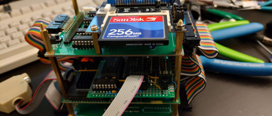
I added some crude functions to the ROM monitor on my Wrap030 project to read the root directory of a FAT16-fomatted disk and load binary files into memory to execute. This opens up a new option for developing programs and running them on the computer, and makes it easier to keep programs on-hand for loading when I demonstrate the computer.
So what new program do I build first for running from disk? The same Mandelbrot renderer I've been using all along, of course! All I needed to do to get it running from disk was adjust a few load instructions to use PC-relative addressing and then change the vasm output to raw binary.
It ran without issue ... mostly. I had been noticing some instability with the system in general. It's not really related to the programming work I've been doing, it just tended to show itself more when doing the kind of FPU-intensive processing required for the Mandelbrot program. Sometimes the system wouldn't boot at all, sometimes it would continually reset. Other times it would run fine for a while, but randomly throw a coprocessor protocol exception (especially when using double- or extended-precision floating point values).
I had a pretty good idea of where this instability was coming from ...
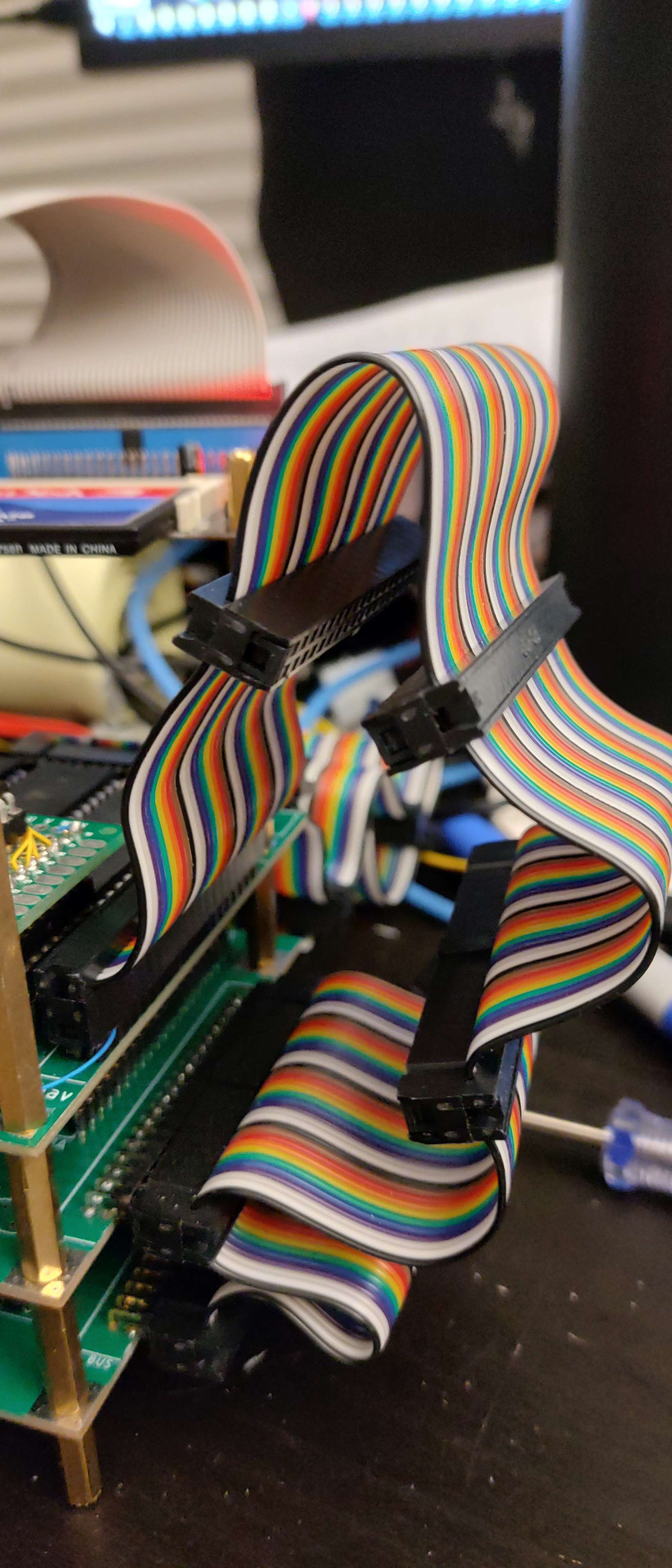
As someone on Discord put it, that's a pretty little antenna I've got there.
High speed computers don't like excessively-long wiring between components. I made the ribbon cables long because there were other boards I developed for this system. But, I'm only using the CPU board, the FPU + IDE mezzanine board, and the video generator board. All that extra wire is just making things more difficult.
A year ago, when I first put these three boards together, I had to bump the bus speed down to 25MHz to get it to run. I could run the CPU board up to 56MHz by itself, and I could get it to run with one expansion board or the other up to 40MHz, but with all three boards, 25MHz was the best I could do (out of the oscillators I had on hand). I have some 33MHz oscillators now, and while I could get it to run sometimes, it was obviously far more unstable.
It was time to trim those pretty little antennas.
I left room for one more card, in case I can get my DRAM card working later, but trimmed a few inches off. The result? Rock solid at 25MHz now.
... and at 32MHz.
... but 40MHz still doesn't run.
I am quite pleased with that result. My target for this system in the beginning was 25MHz. That extra 30% speed increase is very noticeable, especially when running a program like the Mandelbrot renderer.
But I had a thought.
My FPU is rated for 25MHz, and here it's running solid at 32MHz along with the rest of the system. But my FPU board was designed to support the FPU running at a separate clock speed from the rest of the system (the 68881/68882 FPU is actually designed to support this, so I implemented it when I built my mezzanine board).
What would happen if I tried running the FPU even faster? Perhaps using that 40MHz oscillator that I couldn't use for the complete system?
Surprisingly, not a problem running the CPU at 32MHz and the FPU at 40MHz.
... or 50MHz
... or 55MHz
... or 67MHz!
Once again, I've run out of faster oscillators. This computer is running stable with its FPU clocked at over two and a half times its rated speed.
The video above is a real-time capture of the VGA output of this machine running that Mandelbrot renderer (now modified to use 96-bit extended-precision floating-point arithmetic!) with the CPU & main bus clocked at 32MHz and the FPU clocked at 67MHz. Some frames take minutes to render. Some complete in as little as seven seconds.
I am in awe. While I had big dreams when I first started working on this project six years ago, I never could have imagined it running this well at that kind of speed. I am very happy with how this project has turned out so far, and can't quite believe I actually built something like this.
I typically wrap up these posts with a plan of where to take the project next, but the project has already exceeded my expectations. There is so much it is already capable of now that I have a permanent storage option available. I guess I could try getting that DRAM card running to expand the main memory beyond 2MB, or try adding a keyboard and some text routines to complement the video card. Both are good options towards getting a proper operating system running, which has always been a goal of the project.
Either way, I'm sure I'll have fun with it.

#wrap030#mc68030#homebrew computing#retrocomputing#mandelbrot#motorola 68k#motorola 68030#homebrew computer#assembly programming#motorola 68882
18 notes
·
View notes
Text
Logic Planning
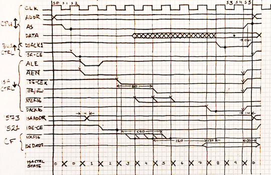
I'm working on adding IDE support to my Wrap030-ATX project.
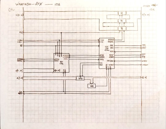
This subsystem is a little complicated, because the CPLD I used for my bus controller didn't have enough I/O pins available to support it. As a result, the logic involves state machines in two different CPLDs working together, plus some additional discrete logic.
To figure out what the timing would look like, I first needed to identify which output signals were necessary for controlling IDE, and all of the input signals that would be used to generate those output signals, as well as the circuits these signals passed through. Instead of working with the complete computer schematic, it was helpful to draw out just the portions that are relevant to this subsystem roughly in input-to-output left-to-right order.
Once I had all of the relevant signals identified and a clear map of their paths through the system, I was able to draw up a timing diagram which follows each signal though time and through the schematic. This shows me when I need to assert specific outputs relative to the state of the various inputs and the system clock, in order to meet setup time requirements for the next stage of the subsystem.
The next step in the process is to plan a finite state machine to handle those signal transitions. Working through the timing diagram, I've determined that the ISA & IDE state machine will need to be clocked on the falling edge of the system clock. I've divided the timing diagram into states starting at each falling edge of the clock.
#wrap030 atx#wrap030#motorola#mc68030#motorola 68k#motorola 68030#homebrew#homebrew computer#retro computing
28 notes
·
View notes
Text
Wrap030-ATX Remembers
No general-purpose computer will do much without a good amount of Random Access Memory for transient storage of code and data. Now that I have confirmed basic operation of CPU, bus controller, ROM, and serial, it's time to turn my attention to main system memory.
Every homebrew computer I've built to date, including previous iterations of the Wrap030 project, has used Static RAM. Static RAM is nearly as simple as peripherals can be — give it an address, assert a Chip Enable and a Read or Write strobe signal, wait a bit, and release. Done, cycle complete. If you don't need to retrieve some data for a good long while, it's no matter so long as the chip still has power. For a small system, SRAM is reliable and dead simple to use.
The problem with SRAM is it is also very expensive. The 2MB of SRAM I had on the previous iteration of Wrap030 cost over $20 — and it's still far from enough to run an operating system like Unix System V, NetBSD, Linux, etc. This is the reason computers generally use Dynamic RAM for primary system memory.
The difference is SRAM uses several transistors to create a flip-flop for storing each and every bit of memory, whereas DRAM uses a capacitor to store each bit of memory. This reduces manufacturing costs and increases storage density, but does come with some trade-offs. Most notably, the capacitors that store bits in DRAM will lose their charge — and the stored data with it — after a rather brief period of time. This means the DRAM capacitors need to be topped off regularly in a process known as a refresh cycle.
Another complication of using DRAM is the bus interface has been changed to allow much larger storage capacities without the physical chip package growing to absurd sizes. Instead of the chip accepting the entire address at once, it expects to be given a Row address (along with a Row Address Strobe [RAS#]) then a Column address (along with a Column Address Strobe [CAS#]), with myriad specific timing requirements for when each signal should be asserted and deasserted.
In short, DRAM is much more difficult to interface with compared to SRAM, so I've never really gotten around to it.
With one of the long term goals of this project being running a *nix operating system though, I'm going to need the larger memory that DRAM affords. So i made provision for a CPLD to serve as a dedicated DRAM controller on the Wrap030-ATX motherboard and added a couple 72-pin SIMM slots. In theory this setup should be able to support up to 256MB of RAM (if rare 128MB SIMMs should fall into my hands...).
So where do we turn when dealing with complicated timing with multiple modes and a bunch of I/O? Why, Finite State Machines, of course! That bit where the DRAM expects a row address for a little while, that's a state. And the following bit where the DRAM expects a column address is another state. And then another state to make sure the DRAM has enough time to write or fetch the data. The round it out with one last state to tell the CPU data is ready.
What about that weird refresh timing? Well, that's just few more states for the state machine. And then one last "idle" state that waits for a refresh timing counter to hit 0 or for the CPU to start a bus cycle. Laid out like that, the DRAM controller became a state machine with 7 or 8 states, a counter, and an address multiplexer.
The logic actually came together easier than expected. Not completely without bugs of course.
There's this note in the datasheets about startup initialization where the DRAM should not be accessed 200μs after power on, and there should be 8 refresh cycles before the first access. Initially I had built this entire sequence into my logic. It consumed a ton of resources and didn't really work right.
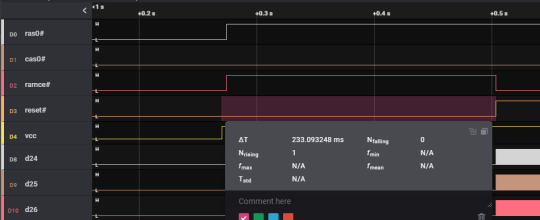
I realized that my reset circuit held the CPU in reset for longer than 200μs on power on, so I was guaranteed that first initialization time. So I removed that startup delay from my DRAM controller logic, and made a few tweaks to the state machine so it could do 8 back-to-back refresh cycles after reset.
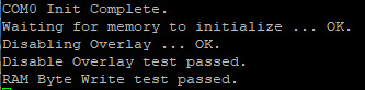
I was able to successfully write to DRAM and read that data back!
That much proved to be the easy part. The next steps were confirming DRAM accesses worked reliably, that I had the order of my byte select signals correct, that I could identify the amount of installed memory, and that all of the installed memory was working. These are programming problems, not logic problems, and I am not a strong programmer. On top of that, not only am I working with unproven DRAM logic, but I'm also using untested SIMMs that I had picked up from Computer Reset.
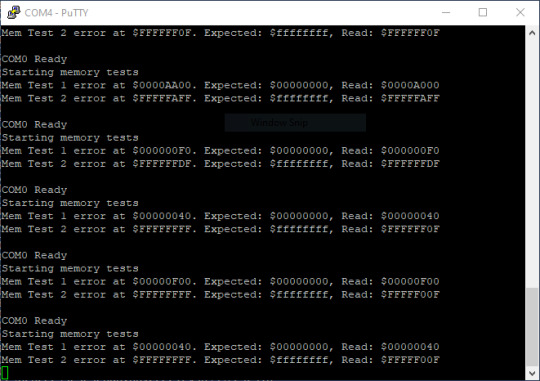
I quickly ran into errors, but was it a problem with my logic? A problem with my timing? A problem with the SIMMs?
I had a large back of 72-pin SIMMs, split fairly evenly between Fast Page Mode (FPM) and Extended Data Output (EDO) types. I tried them all. Some would pass the tests for nearly all addresses but fail at the end. Some seemed to have a stuck bit. Some were just plain bad and gave errors everywhere. It didn't really answer the question about whether my logic was bad, but results were consistent enough for me to think that maybe the logic might be ok.
And then finally I came across a pair of HP-branded 8MB EDO SIMMs that passed a simple write-read test without error ...
... right around the time my serial port stopped working. But the memory test was passing, and I could at least see the serial output on the logic analyzer.
The serial port problem was a bit setback. It had been working but suddenly wasn't. Clearly the UART itself was working, I just wasn't getting anything past the level shifter. Well that at least gave me a starting point of where to look. Sure enough, one of the 12V supply pins was not well soldered. Thankfully a quick fix.
Back to testing memory, I started writing a program to identify the size of the installed SIMM and write a register I added to the DRAM controller to configure the specific geometry of the installed memory. See, DRAM has another lovely quirk — chips of the same size may have a different configuration of Row and Column sizes. For instance one chip may have a 9-bit Column and a 10-bit Row, but the next may have a 10-bit Column and a 9-bit Row, and both are the same size. If the DRAM controller just assumes 12-bit Row and Column (the largest supported by 72-pin SIMMs), then there will be gaps in the memory map that will need to be accounted for in software (using MMU, for example). If the DRAM controller knows the geometry of the installed memory, then it can present the memory to the CPU as one contiguous block of memory.
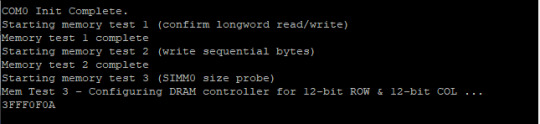
And that's where I found my next bug. The system would just hang when trying to write to that DRAM controller configuration register.
... because I had forgotten to complete that part of the state machine. The result was the state machine would end up in a state for writing to the configuration register, but then it couldn't get out of it. Once I added the missing condition to the state machine logic I was able to correctly identify the geometry and size for my installed memory!
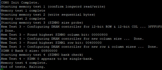
Wow that was long. This has been the biggest, most involved step in the process of bringing up this computer yet. It turns out there are a lot of moving pieces that have to all work together to get the computer running code from ROM and reading/writing DRAM.
Now that I have my main memory working, I should be able to get some software running. I'm hoping to at least have BASIC running in time for VCFSW at the end of June.
#homebrew computing#vintage computing#motorola#mc68030#motorola 68k#assembly programming#motorola 68030#vcf#VCFSW#vcf southwest#verilog#Dynamic RAM#CPLD#troubleshooting#wrap030 atx
33 notes
·
View notes
Text
Failure Unrelated

Someone asked me a question — am I able to separate the bus speed from the CPU speed, since all my logic is synchronous and timing depends on the clock speed?
My initial thought was no, that wouldn't be possible; I didn't design the system that way. The idea got stuck in my head though. I started looking over the board layout and it looked like it might be easier than I initially thought — just cut a trace here, run a bodge there, and build a little adapter board.
... Which of course turned into another cut trace, a few more bodge wires, and a lifted pin on a PLCC socket. But still, the idea seemed solid. I had the CPU and FPU wired to one clock pin, and all of the bus logic was wired to another clock pin. I had an adapter with sockets for two oscillators and a jumper that would let me select whether the bus had its own clock or just used the CPU clock. That last feature was key for testing — I could set the bus to use the CPU clock initially so I could make sure everything was still running the same as before I made any changes.

Fire it up and ... nothing.
Ok, just a loose connection on that PLCC socket. Firm up that connection and try again. This time it boots as expected. I can swap out the oscillator and run the system at different speeds, just like I could before. Time to move the jumper and add a separate bus clock.
Fire it up and ... nothing.
Maybe a different set of oscillators?
... nothing.
Ok, take a step back. Remove the bus oscillator and set the jumper back to run the bus off the CPU clock.
... nothing.
Try a different oscillator, maybe?
... nothing.
Maybe it's that PLCC socket bodge again. I should redo that.
... nothing.
Ok, clearly I've broken something. I'll move those bodges all back to the old primary oscillator pin and remove my adapter board from the mix.
... still nothing.
Time to break out the logic analyzer and see what the heck is going on. Solder some 30 gauge wire to the test points I left on the board — 50mil rectangles of no solder mask on 10mil traces. Add test leads to the top 8 bits of the address bus so I can see what the CPU is trying to access. Add test leads to clock, reset, address & data strobes, bus error, and data strobe acknowledge signals so I can keep track of the start and end of cycles. Then ran a few captures, resetting the system a few times to watch its behavior.

Power comes up, reset triggers, the CPU comes to life and requests the first long word (reset vector) from address $0000,0000. Since I'm running an 8-bit ROM, the bus controller asserts DSACK0#, and the CPU continues fetching bytes until it has the long word. Same thing for the initial stack pointer. The next read is from address $F000,0000, since that is where ROM is located. There's a bus cycle targeting address $E000,0000, which is the first instruction on my ROM (move.b #7,$E0000000). Another 4 cycles targeting ROM for the next instruction long word fetch. Then another 4. It's definitely running code. Then another 4 ... on the fourth access the CPU sits with Address Strobe asserted for nearly 16 microseconds before the bus controller times out and asserts Bus Error.
The CPU tries to read the Bus Error vector. Bus Error. The CPU tries to address the serial port. Bus Error. The CPU tries to read address 0 again. Bus Error. From that point on, every 16 microseconds until the system is reset 6 seconds later ... Bus Error.
That's ... odd. Because the Bus Error can only be asserted by the Bus Controller, and only when the CPU is not addressing ROM or the serial port (since the Bus Controller is responsible for timing accesses to those devices).
I have no idea what is failing, but it does not appear to be the fault of the clock signal. It actually reminds me of a problem I was having when I tried to bring up both the FPU and video chips, where suddenly the bus controller was asserting the UART enable signal when the CPU was addressing the video generator. Perhaps I should take a closer look at my bus controller.
#wrap030 atx#wrap030#motorola#mc68030#motorola 68k#motorola 68030#homebrew computer#homebrew computing#retro computing#troubleshooting
22 notes
·
View notes
Text
Wrap030-ATX Does Something Useful, Runs BASIC

This is it. This is was my goal, where I was hoping to be in time for VCF-Southwest at the end of this month — my Wrap030-ATX project is running the TSMON monitor from ROM; the monitor is loading BASIC from ROM into RAM; and BASIC is running programs.
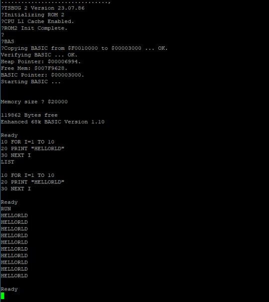
I did run into a few problems getting BASIC running because of all the modifications I've made to it over the years for my 68000 project and the earlier iterations of the Wrap030 project (most problematic being my attempt to modify it to use the FPU).
So I went back and grabbed a fresh copy of the source to work from. I converted the syntax from VASM to GNU AS, swapped out the M6850 ACIA UART routines for new ones using the 16c550 UART, and updated the addresses in the program and my linker script for the Wrap030-ATX memory map. It took a few tries to get it running, but I think the results really speak for themselves.
Now that I've met my minimum goal ahead of VCFSW, everything else is extra. I do want to see if I can get the FPU and my video generator working.
#wrap030 atx#retro computing#motorola 68k#mc68030#motorola#assembly programming#motorola 68030#basic programming#homebrew computer#homebrew computing#vcf southwest#VCFSW
23 notes
·
View notes
Text
Wrap030-ATX First Code
This is a big step forward — Wrap030-ATX, my microATX form factor 68030-based homebrew computer, is running code from ROM. Externally, all it's doing is blinking an LED, but that LED is software-controlled, with a sizable delay loop between blinks to make it something that is human-visible.
Getting to this point took quite a bit of work after the free run tests. Nearly all of the logic on this project is in CPLDs. Of note here is the primary bus controller, which handles access timing, bus cycle termination, and a settings register.
For the computer to run code, it has to be able to read from ROM. Reading from ROM requires the bus controller to decode the CPU address, assert the ROM's Chip Enable (CE#) and Output Enable (OE#) signals, wait the appropriate length of time for the ROM to output stable data on the bus, and then assert the appropriate bus cycle termination signal for an 8-bit peripheral (DSACK0#).
Once I had the minimal functionality for ROM access cycles, I was able to repeat the free run test, but this time with only the to 8 bits of the data bus (D[31:24]) pulled low.
Once I confirmed the ROM access cycle logic was working, I added the bus controller register access cycle logic. The bus controller has a single settings register that will control the Debug LED, startup ROM overlay, and ATX soft power. The CPU will need to be able to write to this register, and reading from it is helpful as well.
The bus controller logic is fully synchronous and managed by a state machine, so all that was needed to add the settings register was a couple new states for the state machine — one for read and one for write.
Put all that together, and we have a computer that can run the most basic of programs, with just a single LED for output.
The next thing I need to get working is a serial port. Everything that comes after this point will be a lot easier if I can output helpful debugging messages over serial.
#homebrew computing#motorola#mc68030#motorola 68k#verilog#cpld#motorola 68030#assembly programming#wrap030 atx#retro computing
26 notes
·
View notes
Text
Wrap030-ATX Says "Hellorld"

In the immortal word of [Usagi Electric], Wrap030-ATX says, "Hellorld". This can only mean one thing — serial I/O is working!
Getting serial working should be relatively straightforward. The UART I'm using is an 8-bit peripheral which needs a Chip Enable and an Output Enable signal, just like the ROM. It's a little slower, so it will need an extra wait state or two, but it should be easy enough to modify the bus controller state machine to address the UART as well. It didn't take me long to add the necessary logic, solder on the new parts, and fire it up for a test run.
Nothing happened.
I went through all the normal steps — double check the wiring, make sure my test leads haven't come loose, make sure the chip is seated properly in its socket and not shorted out …
… I burned my finger. And not just a little 'ow that's a bit warm to the touch', but a proper second-degree burn. That UART chip was hot.
That kind of heat can only mean there is a direct short somewhere in the chip. It could just be a defective part, but since they are out of production and I only have a few on hand, the best thing to do is confirm the problem isn't on my board somewhere before trying another one (and potentially destroying it too).
The PCB layout passed Design Rule Check, so I didn't have any overlapping traces. The schematic didn't have any obvious errors where maybe I had inadvertently tied an output signal to power or ground. This was not an existing library part — it was one that I had to create — so it was possible I had gotten pin assignments wrong.
I pulled up the datasheet and opened the part in the library and started confirming all of the pin assignments matched the datasheet. Bus & I/O pins were all fine; but the very last power supply pin was assigned to Vcc, where the datasheet had it marked Vss. So I had a +5V power supply capable of sourcing in excess of 25A of current running into what should have been a ground pin. No wonder it was hot enough to burn; it's a wonder it didn't release the magic smoke immediately.
This is a challenge. I need to swap a power pin for a ground pin on a PLCC socket. On a simpler project, I might've gotten away with just cutting the trace running to that pin and soldering a bodge wire to it.
… But this is a 4-layer board. There is no mere trace running to that pin — there is an entire inner layer attached to it. My best bet would probably be removing the offending pin from the socket, but depending on how it's constructed, I may not be able to remove the pin.
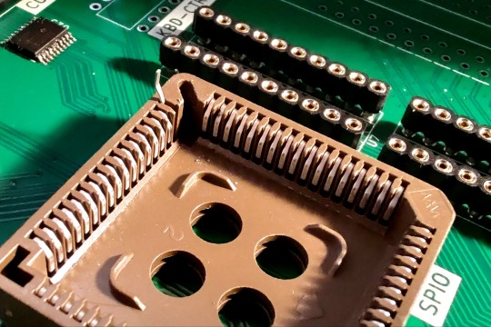
Through-hole PLCC socket pins are staggered. Some go straight down through the board, but alternating pins make an L-shape so that the socket can have two rows of through-hole pins at a 0.1" grid spacing. The L-shaped pins would be trapped under the plastic base of the socket.
Luckily, the pin in question was the first on its side, so it went straight through the base. I started by bending up its contact, and then with the heat turned up on my soldering iron, I was able to pull it out of the board and completely free from the socket.
I had some wire on hand that was just the right width to match the slots for the contacts in the socket. I bent a flat loop to make contact with the chip lead and shoved it down into the slot. It worked perfectly. I ran it over to a nearby jumper that had a ground lead, and there I have my first bodge wire for this project.
It still didn't work.
This is the part of debugging that is the most frustrating. There's a problem and it takes a considerable amount of effort to identify not just the cause, but also the solution. And then after working through those steps and finally implementing a fix, it still doesn't work because there is another problem. Back to square 1 with debugging.
Why is it not working? It's not burning hot, so that problem was indeed solved. I'm getting data to the chip, and the read/write strobes are functional. The chip select signals are ... wait, why isn't chip select working?
... Because I forgot a chip, that's why. Insert Picard facepalm GIF here.
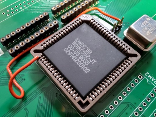
The UART I'm using is a Western Digital WD16C552. It's a lovely chip designed for 386 era PCs contain two 16550-compatible UARTs and a Centronics Parallel port as well. It is three peripherals in one package. To save I/O on my bus controller CPLD, I used a 74'139 2-to-4 decoder to further break down the address for this serial/parallel I/O chip into the three specific peripheral select signals I needed. And I simply forgot to solder that chip onto the board.
Two headers and one 74LS139 later and finally my terminal came to life. The Wrap030-ATX whispered its very first greeting, "HELLORLD". Serial I/O is working and I can move on to the next step. And oddly enough, I tested that first chip that flirted with fire and it actually still works!
I am racing forward through the countless tests and steps to bring this machine to life ahead of VCF Southwest at the end of June. I am hoping to get it at least running BASIC over serial by that time, but for that I am going to need some RAM. This will be fun because this is my first time actually building a DRAM controller; I've done some test designs before but never actually built them. Fingers crossed I don't run into any show-stopping errors getting it up and running.
#homebrew computing#mc68030#motorola#motorola 68k#motorola 68030#vintage computing#vcf southwest#wrap030 atx#western digital
21 notes
·
View notes
Text
Introducing Wrap030-ATX
New Boards Day!

They're here!
This is a project that has been a long time coming, and something I have wanted to do for a long time.
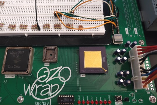
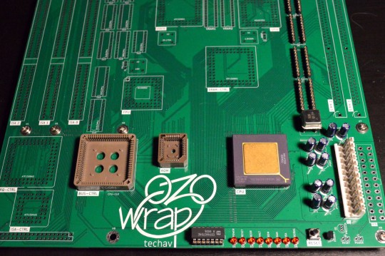
This is the largest, most complex PCB I have ever designed — a 9.6x9.6 inch (244x244mm) square, 4-layer, complete motherboard for my MC68030 homebrew computer project.
It is designed to support the Motorola MC68030 CPU, MC68882 FPU, two 72-pin SIMM sockets, 512kB ROM, two serial ports, one parallel port, PS/2 keyboard, 4-bpp VGA video, IDE hard drive, and three ISA expansion slots. A complete system all in a microATX form factor.
This builds on my previous work with the 68030, based heavily on my wire-wrap project and the boards that followed. It's a project over four years in the making. I have made a few improvements on the old design, like 16550-compatible serial ports and an updated memory map to support much more RAM in a contiguous space.
Keeping with my existing system designs, I've combined most of the logic into a set of CPLDs. This makes things like PCB layout and logic debugging so much easier. Most of the remaining discrete logic on the board is 74'245 bus transceivers for driving memory and the ISA slots.
I've kept the name "wrap030" in honor of the project's origin as a wire-wrapped prototype, despite the move to proper PCBs. It's just what I've been calling the project in my own head (and design files) all this time, so at this point no other name would feel right.
I of course wasted no time starting to assemble one, but I did stop myself from getting too carried away with the soldering iron. I want to be methodical and test each section before moving on to the next.
I have already found one major error in my board layout — the footprint for the VGA connector is backwards. I may need to bodge together some kind of adapter.
So far I've confirmed the minimalist AT power supply section works with no major shorts on power supply rails, and the reset circuit is working as expected. Next step is to try a free run test with the CPU to ensure the system clock and CPU are working. Once that is confirmed working, I can start loading logic for accessing ROM. My goal is to have it at least running BASIC on a serial terminal by VCFSW in June.
I've forked my existing wrap030 repository on GitHub for this new Wrap030-ATX, since it does make some breaking changes that will require updates to logic and programs. New repo is here:
#homebrew computing#mc68030#motorola#motorola 68k#motorola 68030#vintage computing#jlcpcb#vcf southwest#wrap030-atx
32 notes
·
View notes
Text
Extra Thinky Bits

Ever since I built my 68000 computer, I've used a BASIC Mandelbrot rendering program I got from RosettaCode as a test benchmark. On the 6MHz 68000 it took nearly 10 minutes to run. With the 68030 running at 56MHz using a 32-bit data bus with L1 cache enabled, the same BASIC program completed in around 14 seconds.
But we can do better. EhBASIC is written in assembly to use 32-bit single-precision floating point numbers internally, but all of its mathematical routines use the CPU's integer ALU. There are large sections of code that could theoretically be replaced by single instructions for the 68882 floating point math coprocessor (FPU).
Adding the FPU is where I stopped on my original wire-wrapped prototype. I simply never could get it working reliably. I've since learned that I had some logic errors that were probably causing more trouble than my chosen method of prototyping. But this meant it was probably best to start over, and if I'm starting over, a custom PCB with a CPLD to handle logic & timing would be much easier, much more flexible, and much more reliable.
Another tumblr user, Avics1967, had pointed out that logic error to me a while back. It turns out the 68882 FPU is picky about the setup time relationship between the FPU's Chip Select signal and the CPU's Address Strobe signal. Basically, the Chip Select signal can't be transitioning at the same time that the Address Strobe signal is falling, and there's a few nanoseconds on either side of that AS# transition where the CS# signal must be stable. My original design didn't take this into account.
This setup time target ended up being harder to hit than I anticipated. With my little system running at 40MHz, there is just 12.5ns between the CPU asserting the address bus and the CPU asserting its Address Strobe. I need to allow about 3ns for the FPU Chip Select signal to be stable before AS# falls.
I'm using a 10ns CPLD for logic.
My first draft for the logic also did not meet timing requirements, and with my bus speed and parts on hand it never would. Luckily, the 68882 also supports what Motorola called "Late Chip Select", where the CS# signal could be asserted after AS#. So that's what I ended up doing — I implement a delay synchronous to the CPU clock to assert CS# half a clock after AS#.
I ran into an interesting problem while testing though. I assembled a short program to add 2+3 and store the result in memory where I could check if the result of 5 was stored properly. What I got instead was an endless chain of bus errors. If I hit reset quickly enough I could see the very first error was actually an Address Error, and then came the endless chain of Bus Errors.
This made no sense. The FPU can generate some exceptions, like the Coprocessor Protocol Violation I had gotten with my last prototype. And if there was a problem with my logic, a Bus Error might be thrown if the FPU wasn't detected or didn't respond in time. But an Address Error?
Turns out the FPU wasn't the problem at all. There was a typo — a single missing # — in my monitor which caused the CPU to try to load an odd instruction as a pointer instead of the actual pointer to the exception handler routine. So something was indeed causing an exception, but I couldn't see what the exception actually was because it was immediately followed by an Address Error which also spawned a Bus Error.
Thankfully, my exception table is in RAM, so I was able to patch it live before running my test program. And the next time I tried testing the FPU? It worked!
I have no idea what was causing the initial exception, but the FPU has been working for me since.
Now it's time to write some more sophisticated programs to really test the FPU, and maybe modify BASIC to use the FPU instead of its built-in arithmetic functions.
37 notes
·
View notes
Text
Wrap030-ATX First Tests
The best place to start with assembling and testing a board like this is the power supply. If there's a catastrophic error, like a direct short between supply rails, it's best to find out before wasting other components. Thankfully on this project, I'm using a standard PC power supply so all I need is some basic filtering capacitors. Not much to screw up there except maybe some backwards electrolytics.
Next is generally reset and CPU clock. These are essential for getting the CPU up and running and should be confirmed operational before continuing. Here again I'm using stock modular components — a brownout reset signal generator and a can oscillator — so debugging was minimal.
Finally, the CPU should be tested with these signals to see if it will free run (tie the CPU data bus to a known value, usually something like 0b00000000, and watching to see if the address bus increments freely).

The CPU free run test is an important one. It confirms the most basic functions of the board and the CPU are functional. A board that can't free run at this stage likely has some significant problem that must be solved before anything else will work.
Luckily, it passed this test!
I used the data bus transceiver sockets to attach test wires to, so I could tie all the data bus signals low. On the 68k architecture, $0000,0000 corresponds to the instruction ORI.b #0,D0 which is a 16-bit opcode ($0000) for an OR instruction followed by an immediate constant word ($0000). So for every 32-bit bus access, the CPU is fetching one complete instruction, incrementing the Program Counter by 4, then repeating. The result of the instruction is stored in the D0 register, so nothing is ever written to the bus.
This behaviour can be confirmed with a logic analyzer, but it's easiest to visualize by connecting LEDs to some of the higher address bits and watching them count up in binary (which is what I did here).
On the 68030 there is a bit more to do than just grounding the data bus. In particular, the CPU's asynchronous bus expects peripherals to report they are ready and have placed valid data on the bus by asserting the Data Strobe Acknowledge signals (DSACKn#). In normal operation, the system will delay asserting these signals to give the peripheral device enough time to do its job, signalling the CPU to insert wait states until the data is ready. For free run though, these signals can be tied low to signal to the CPU that the data it's requesting (all 0s) is ready immediately (because the data bus is tied to ground).
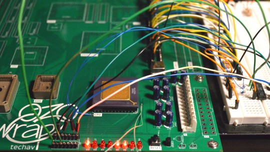
Here is where a last-minute addition to my PCB layout really came in handy. I removed the solder mask on these small sections of important signal traces so I would have a clear place to probe these signals on the top of the board. This also gave me just enough room to solder some 30 gauge wire to the DSACKn# and address signals for running the free run test.
Now that I know the most basic functions of the board are working, I can move on to the next step — running first code. To run real code I'll need ROM working, which will also require the bus controller CPLD to be minimally functional.
I am hoping to have this project at least running BASIC in time to exhibit it at VCF Southwest in Dallas at the end of June this year. I've got a lot of work still to do to reach that goal, but passing these first tests does give me hope that there are no huge show-stopping problems with my PCB (at least nothing that can't be worked around with a bodge wire or two)
#homebrew computing#vintage computing#wrap030 atx#motorola#mc68030#motorola 68k#motorola 68030#vcf southwest#VCFSW
13 notes
·
View notes
Text
Full Speed Ahead ... Finally
I have been building my 68030 computer around a 25MHz-rated part, so that has always been my target. My original wire-wrap prototype initially ran at half that, but as I continued to expand the project, the best I could manage was 6MHz. Eventually, the whole thing got so unstable I had to abandon plans to continue adding FPU, DRAM, IDE, etc.
I do still want to add those parts to the project, to learn more about working with them. That's why I ordered the custom PCBs — I was hoping a PCB would be a more stable platform for future expansion and allow me to finally run the machine at the 25MHz target.
Once I got the new PCB prototype working I tried again with a 25MHz oscillator (my new glue logic no longer divides the clock like my original).
It didn't work.
In fact, at 25MHz it failed in the same way it always had on the old wire-wrap prototype. It seemed 12 MHz was my limit.
Or was it? Maybe I just had a bad oscillator. Perhaps a new one would work better?
A ridiculous line of thought, given that the 25MHz oscillator I had did indeed run the computer at one time. But, I did want to see how fast I could get it to run, and there are some respectable speeds between 12MHz and 25MHz. So I placed an order for a few oscillators, 16MHz, 20MHz, 24MHz ... I also stocked up on some common resistors and capacitors to make the most of the shipping fee.
Got the new parts in, threw on the 24MHz oscillator and ... nothing. It didn't work.
There is a problem I noticed when I did my original troubleshooting on this PCB — some of the wired-or signals had very slow rise times. I don't have a proper oscilloscope, so it's hard to tell sometimes if analog problems like that are measurement error or induced by stray capacitance of the measurement leads. But, the 8kΩ resistor networks I had gotten from surplus to use as pull-ups on this project were a bit high. Perhaps a lower-value pull-up resistor might help here.
Among the resistors I ordered were some 4.7kΩ and 1kΩ resistor networks. 4k7 is a fairly standard pull-up value, and some rough math had shown 1k might be a good value for this project. So I swapped out the 8k resistor networks for the new 1k networks and gave it a shot. It still ran without issue at 12MHz...
And at 16MHz.
And at 20MHz.
And at 24MHz.
And at 25MHz.
And at 32MHz.
And at 40MHz.
My MC68030 rated for 25MHz was running BASIC stable at a 60% overclock. Even the RAM was overclocked at this point, with cycles reduced to 50ns for SRAM rated for 55ns. It would seem that all this time my choice of pull-up resistor value had as much or more to do with my speed limits as the method of prototyping.
It wasn't perfect though, and as soon as I added my SE-VGA card back into the mix it would no longer successfully load BASIC at 40MHz. It did however run just fine at 32MHz, even with the SE-VGA card.
Ludicrous Speed
In the years since I started this project I acquired another 68030 CPU — a 40MHz-rated 68EC030 (the EC units lacking the on-board MMU). I'm sure you can see where this is going.
First, I needed to modify my glue logic. RAM access cycles were going to need another wait state, ROM another two. While I was at it, I created a new cycle specifically for my SE-VGA card, with three wait states. Since my UART (68B50) is actually rated for 2MHz, and my timing was originally factored for 1MHz with a 25MHz base clock, I left the UART timing alone to push it closer to its rated speed. All-around, the new timing should support up to 50MHz base clock.
New logic, everything ran fine at 32MHz. Swapped in the EC030 and no problems. Time to see how fast it will go.
40MHz, no sweat
50MHz, still running cool
56MHz, no problems
I'm out of oscillators. My 68030 homebrew, with a 40MHz-rated EC030 is running reliably at 56MHz, a 40% overclock. Even the SE-VGA card is working, and much happier with its custom timing added to the glue logic.
I've been using a simple Mandelbrot rendering BASIC program as a benchmark. On my original 6MHz 68000 build, this program takes around 9 minutes to complete. When I first ran it on the 68030, running at 12MHz, with cache disabled, and BASIC in 8-bit ROM, it took just under 5 minutes. Now, with BASIC running from RAM on the 32-bit bus, L1 cache enabled, and CPU at 56MHz, the Mandelbrot program completes in 14 seconds. That is an incredible performance increase for a simple homebrew computer.
It does generate some heat now, so I added a small heatsink to the CPU to be safe. Current consumption for the system is up 300mA just from raising the clock speed.
Motorola originally sold 68030 CPUs rated as high as 50MHz. I wonder if my later production units just benefit from what they learned pushing the architecture that high, or if it's reflective of what the CPU can handle in general. Could I push a 50MHz part up 40%? A 70MHz 68030 homebrew certainly would be interesting.
56 notes
·
View notes
Last Seen Blogs

mushroomheadcoc
Sin título

2die4
Unlucky Scorpio

sampurnasuvidhakendra
Sampurna Suvidha Kendra

piipstachio
Morningstar

grimmichibigbang
GrimmIchi 2021 Big Bang