#nanoworld
Text
2 notes
·
View notes
Photo
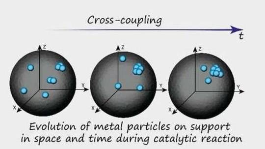
Chemists find that metal atoms play key role in fine organic synthesis
A small team of chemists at the Russian Academy of Sciences, has found that metal atoms, not nanoparticles, play the key role in catalysts used in fine organic synthesis. In the study, reported in the Journal of the American Chemical Society, the group used multiple types of electron microscopy to track a region of a catalyst during a reaction to learn more about how it was proceeding.
Prior research has shown that there are two main methods for studying a reaction. The first is the most basic: As ingredients are added, the reaction is simply observed and/or measured. This can be facilitated through use of high-speed cameras. This approach will not work with nanoscale reactions, of course. In such cases, chemists use a second method: They attempt to capture the state of all the components before and after the reaction and then compare them to learn more about what happened.
This second approach leaves much to be desired, however, as there is no way to prove that the objects under study correspond with one another. In recent years, chemists have been working on a new approach: Following the action of a single particle during the reaction. This new method has proven to have merit but it has limitations as well—it also cannot be used for reactions that occur in the nanoworld. In this new effort, the researchers used multiple types of electron microscopy coupled with machine-learning algorithms.
Read more.
#Materials Science#Science#Atoms#Metals#Catalysts#Materials synthesis#Organic materials#Electron microscopy#Reactions#Nanotechnology#Machine learning#Palladium
18 notes
·
View notes
Text
Unveiling the Best TEM at Wintech Nano-Technology Services Pte Ltd
In the realm of nano-technology, precision and clarity are paramount. At Wintech Nano-Technology Services Pte Ltd, our commitment to excellence is epitomized by the cutting-edge tools we employ. Among these, best TEM one shines brightly as the cornerstone of our analytical prowess – our Transmission Electron Microscope (TEM).
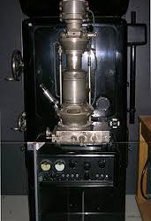
TEM, short for Transmission Electron Microscope, stands as the linchpin of our analytical arsenal. Its unparalleled ability to unveil the intricate details of nanomaterials makes it an indispensable tool in our quest for scientific advancement. Let us delve deeper into what sets our TEM apart and why it stands as the best in class.
Unmatched Resolution
In the realm of nano-technology, every atom matters. Our TEM boasts an unrivaled resolution that enables us to visualize structures with atomic precision. Whether it's studying the morphology of nanoparticles or analyzing crystal defects at the atomic scale, our TEM delivers images with breathtaking clarity, empowering our researchers to unravel the mysteries of the nanoworld.
Advanced Imaging Techniques
Equipped with a myriad of imaging techniques, our TEM transcends conventional microscopy. From high-resolution imaging to electron diffraction and elemental mapping, our instrument offers a comprehensive suite of capabilities that cater to diverse research needs. Whether it's discerning the composition of a complex nanostructure or probing its electronic properties, our TEM stands ready to illuminate the path forward.
Dynamic In Situ Capabilities
Understanding dynamic processes at the nanoscale requires real-time observations. Our TEM's in situ capabilities enable us to witness phenomena as they unfold, capturing elusive details that would otherwise remain hidden. Whether it's tracking the growth of nanomaterials or studying their behavior under varying conditions, our TEM provides a window into the dynamic nature of nanostructures, opening new avenues for exploration.
Collaborative Platform
At Wintech Nano-Technology Services Pte Ltd, we recognize the power of collaboration in driving innovation. Our TEM serves as a collaborative platform, fostering interdisciplinary research endeavors that transcend traditional boundaries. Whether it's partnering with academia, industry, or fellow researchers, our TEM serves as a catalyst for transformative discoveries, propelling the field of nano-technology forward.
Commitment to Excellence
Behind every groundbreaking discovery lies a team of dedicated professionals. At Wintech Nano-Technology Services Pte Ltd, our TEM is supported by a team of experts who are committed to excellence in every facet of their work. From instrument maintenance to data analysis, our team ensures that our TEM operates at peak performance, empowering researchers to push the boundaries of what's possible in nano-technology.
In conclusion, the TEM at Wintech Nano-Technology Services Pte Ltd stands as a beacon of innovation in the field of nano-technology. With its unmatched resolution, advanced imaging techniques, dynamic in situ capabilities, and collaborative platform, our TEM embodies excellence in every sense. As we continue our journey of scientific discovery, rest assured that our TEM will remain at the forefront, illuminating the path to a brighter, nano-enabled future.know more
0 notes
Text
Unveiling the Nanoscale A Comprehensive Guide to TEM Analysis in WinTech Nano
Introduction: In the realm of nanotechnology, understanding materials at the atomic and molecular levels is essential for innovation and advancement. Transmission Electron Microscopy (TEM) stands as a powerful tool, allowing researchers to delve deep into the nano world. best TEM In this blog, we'll explore the intricacies of TEM analysis, particularly in the context of WinTech Nano, and how it enables groundbreaking discoveries in various fields.
Understanding TEM: Transmission Electron Microscopy (TEM) is a microscopy technique where a beam of electrons passes through an ultra-thin specimen, interacting with the sample as it traverses. Unlike traditional light microscopes, TEM employs electrons, which have much shorter wavelengths, enabling significantly higher resolution imaging. This technique offers unparalleled insights into the structure, morphology, and composition of materials at the nanoscale.
The Role of WinTech Nano: WinTech Nano is a cutting-edge software suite designed to complement TEM analysis, providing researchers with advanced tools for data acquisition, processing, and interpretation. Its intuitive interface coupled with powerful analytical capabilities makes it a preferred choice in the nanotechnology community.
Key Features of WinTech Nano:
Image Acquisition: WinTech Nano facilitates high-resolution imaging, allowing researchers to capture detailed micrographs of their specimens. It supports various imaging modes, including bright-field, dark-field, and high-angle annular dark-field (HAADF), each offering unique insights into sample characteristics.
Spectroscopy and Elemental Analysis: With WinTech Nano, elemental analysis becomes seamless. Energy-dispersive X-ray spectroscopy (EDS) capabilities integrated into the software enable researchers to identify and quantify elemental compositions within their samples accurately.
Crystallography and Phase Analysis: Characterizing crystal structures and phases is fundamental in materials science. WinTech Nano streamlines crystallographic analysis, enabling researchers to determine lattice parameters, grain orientation, and phase distributions with precision.
In-situ Experiments: WinTech Nano supports in-situ experiments, allowing researchers to observe dynamic processes in real-time. Whether it's studying phase transformations, nanoparticle growth, or mechanical properties, WinTech Nano facilitates comprehensive data acquisition and analysis.
Applications of TEM Analysis in WinTech Nano:
Nanomaterials Synthesis: Understanding the nucleation and growth mechanisms of nanomaterials is crucial for tailoring their properties. TEM analysis in WinTech Nano aids in elucidating the morphology, size distribution, and crystal structure of synthesized nanoparticles.
Semiconductor Devices: In the semiconductor industry, precise characterization of device structures is paramount for optimizing performance. WinTech Nano enables researchers to analyze defects, interfaces, and dopant distributions in semiconductor devices with unparalleled detail.
Biological Imaging: TEM plays a pivotal role in elucidating the ultrastructure of biological specimens. With WinTech Nano, researchers can visualize cellular organelles, protein complexes, and viral particles at the nanoscale, advancing our understanding of biological processes.
Conclusion: Transmission Electron Microscopy coupled with WinTech Nano empowers researchers to explore the nanoworld with unprecedented clarity and detail. By leveraging its advanced imaging, spectroscopic, and analytical capabilities, scientists can unravel the mysteries of nanomaterials, semiconductor devices, biological systems, and beyond. As technology continues to evolve, TEM analysis in WinTech Nano will undoubtedly remain at the forefront of nanoscience research, driving innovation and discovery for years to come.read more.
0 notes
Text
🌟 Quantum Dots Lighting Up the Tech Scene! 🚀✨
Hey Quantum Enthusiasts! 🌈✨ Did you know that the Quantum Dot Sensor Market is the new shining star in the tech galaxy? 🌌🔍 Let's dive into the quantum realm and explore the incredible potential of these tiny yet mighty sensors! 🌐💡
🔬 What are Quantum Dot Sensors? 🤔💡 Quantum Dots are like the rockstars of the nanoworld! 🎸✨ These minuscule semiconductor particles are changing the game in sensor technology. They're boosting image quality, enhancing color accuracy, and taking performance to a whole new level! 🚀🔍
💡 Brightening Up Displays! 🌈🖥️ Say goodbye to dull screens and hello to vibrant, true-to-life colors! 🌟 Quantum Dot Sensors are revolutionizing display technology, giving you an immersive visual experience like never before! 🎨🔮
📸 Picture-Perfect Moments! 📷✨ Capture every detail with precision! Quantum Dot Sensors are elevating camera capabilities, making your photos sharper, clearer, and more vivid! 📸🌠 Get ready to be the photography pro in your squad! 🤩🌟
🌐 Quantum Dot Market Boom! 💥💰 The market for Quantum Dot Sensors is skyrocketing, and tech giants are all aboard the quantum hype train! 🚂🌌 Brace yourselves for a tech revolution that will reshape how we see and capture the world! 🚀🌐
🚀 Future Tech in the Palm of Your Hands! 🌐📱 Imagine holding the power of quantum technology in your hands! The Quantum Dot Sensor Market is paving the way for a future where cutting-edge tech becomes an everyday marvel! 🌈🔮
Ready to embrace the quantum leap? 🚀🌌 Strap in, tech enthusiasts, because the Quantum Dot Sensor Market is set to redefine the way we experience the world! 🌐✨ #QuantumRevolution #TechMarvels #QuantumDotSensors 🚀🔍
0 notes
Text
AFM Probe Market Detailed Strategies, Competitive Landscaping and Developments for next 5 years
Latest released the research study on Global AFM Probe Market, offers a detailed overview of the factors influencing the global business scope. AFM Probe Market research report shows the latest market insights, current situation analysis with upcoming trends and breakdown of the products and services. The report provides key statistics on the market status, size, share, growth factors of the AFM Probe The study covers emerging player’s data, including: competitive landscape, sales, revenue and global market share of top manufacturers are Team Nanotec GmbH (Germany), Olympus Corporation (Japan), Bruker (United States), Asylum Research (Oxford Instruments) (United States), Applied NanoStructures, Inc. (United States), NT-MDT (Russia), NanoWorld AG (Switzerland), Hitachi (Japan), Horiba (Japan), Nanonics Imaging (Israel)
Free Sample Report + All Related Graphs & Charts @: https://www.advancemarketanalytics.com/sample-report/648-global-afm-probe-market?utm_source=Organic&utm_medium=Vinay
AFM Probe Market Definition:
AFM(Atomic-force microscopy) is a type of scanning probe microscopy (SPM). The AFM is really in the cantilever/tip assembly which is referred to as the probe. The probe really has two parts such as the cantilever and the tip. The dimensions of the cantilever are on the scale of micrometers. The radius of the tip is usually on the scale of a few nanometers to a few tens of nanometers.
Thanks for reading this article; you can also get individual chapter wise section or region wise report version like North America, Europe or Southeast Asia.
0 notes
Text
Unveiling the Marvels of Nanotube Bottles: A Miniature Engineering Wonder
Greetings, curious minds of the internet! Today, we're diving headfirst into the fascinating world of Nanotube Bottles. You might be wondering, "What in the nanoworld are those?" Well, buckle up, because we're about to embark on a journey through the science behind these miniature marvels of engineering.
The Intriguing World of Nanotube Bottles
Nanotube Bottles might sound like something out of a sci-fi movie, but they're very much a reality. These remarkable creations are a testament to the incredible advancements in nanotechnology. Let's start by understanding the basics.
What Are Nanotube Bottles?
Imagine tiny, cylindrical structures with walls so thin that they're made up of a single layer of carbon atoms. These are carbon nanotubes, and when they are shaped into bottle-like structures, we get Nanotube Bottles. These minuscule containers can hold and transport a variety of substances, and their potential applications are vast.
The Magic of Nanotube Powder
To grasp the science behind Nanotube Bottles, we need to take a closer look at their core component: nanotube powder.
What Is Nanotube Powder?
Nanotube powder consists of an assembly of carbon nanotubes. These tubes are incredibly small, with diameters on the nanometer scale, but their lengths can range from micrometers to millimeters.
- The powder is created through various techniques like chemical vapor deposition or arc discharge methods. These methods allow precise control over the size and properties of the carbon nanotubes.
Why Nanotube Powder?
Nanotube powder is the raw material for crafting Nanotube Bottles. It's the building block, much like bricks are for a house. The remarkable characteristics of carbon nanotubes make them ideal for this purpose.
- Their immense strength, high electrical conductivity, and unique chemical properties make them an engineering marvel.
Crafting Nanotube Bottles
Creating Nanotube Bottles is no walk in the park. It involves several intricate steps that require finesse and precision.
Step 1: Nanotube Growth
To kickstart the process, carbon nanotubes are grown using a catalyst, often made of transition metals.
The structure of these tubes is manipulated to create the desired bottle shape. This involves controlling the growth conditions carefully.
Step 2: Bottle Formation
Once the nanotubes reach the desired length, they are carefully sealed at one end to form a closed bottle-like structure.
It's almost like creating a tiny, nanoscale message in a bottle!
Step 3: Functionalization
To make Nanotube Bottles practical, they are often functionalized. This means adding specific molecules or substances to their interior, which can serve a variety of purposes, from drug delivery to targeted chemical reactions.
Applications and Future Prospects
Nanotube Bottles hold incredible promise and have already found applications in various fields. Here are some exciting prospects:
Drug Delivery: These tiny vessels can transport medications to precise locations within the body, minimizing side effects.
Chemical Sensing: Nanotube Bottles can be used to detect specific chemicals or toxins, making them invaluable for environmental monitoring.
Nano-Reaction Vessels: With their minute size and precise control, they are ideal for conducting chemical reactions on a nanoscale.
Conclusion
In the realm of nanotechnology, Nanotube Bottles are a true marvel of engineering. Their tiny size conceals immense potential, and as we continue to unlock the secrets of the nanoworld, we can only anticipate more innovative applications for these miniature wonders. Whether it's revolutionizing drug delivery or enabling groundbreaking chemical research, these tiny bottles have the power to change the world in ways we're only beginning to fathom.
So there you have it – a glimpse into the science behind Nanotube Bottles. The future holds endless possibilities for these miniature marvels, and I, for one, can't wait to see where this remarkable journey takes us!
0 notes
Text
NYTimes: Nobel Prize in Chemistry Awarded to 3 Scientists for Exploring the Nanoworld
Nobel Prize in Chemistry Awarded to 3 Scientists for Exploring the Nanoworld https://www.nytimes.com/2023/10/04/science/nobel-prize-chemistry.html?smid=nytcore-android-share
0 notes
Text
The new laureates discovered and developed quantum dots, semiconductors made of particles squeezed so small that their electrons barely have room to breathe.
Nobel Prize in Chemistry Awarded to 3 Scientists for Exploring the Nanoworld, NYTimes
0 notes
Text
Nobel Prize in Chemistry Awarded To 3 Scientists for Exploring the Nanoworld
http://i.securitythinkingcap.com/Sx0Zzy
0 notes
Text
I have done high pressure studies and at a later point NMR experiments. But NMR under pressure sounds scary ...
Moreover, it's about intrinsic disorder in a cold shock protein, so I really should read this paper ...
Paper is here (open access):
https://onlinelibrary.wiley.com/doi/10.1002/anie.202401343
0 notes
Link
A team of scientists, led by researchers from the Max Born Institute in Berlin and Helmholtz-Zentrum Berlin in Germany and from Brookhaven National Laboratory and the Massachusetts Institute of Technology in the United States has developed a revolutionary new method for capturing high-resolution images of fluctuations in materials at the nanoscale using powerful X-ray sources. The technique, which they call Coherent Correlation Imaging (CCI), allows for the creation of sharp, detailed movies without damaging the sample by excessive radiation. By using an algorithm to detect patterns in underexposed images, CCI opens paths to previously inaccessible information. The team demonstrated CCI on samples made of thin magnetic layers, and their results have been published in Nature.
The microscopic realm of the world is constantly in motion and marked by unceasing alteration. Even in seemingly unchanging solid materials, these fluctuations can give rise to unusual properties; one example being the lossless transmission of electrical current in high-temperature superconductors. Fluctuations are particularly pronounced during phase transitions, where a material changes its state, such as from solid to liquid during melting. Scientists also investigate very different phase transitions, such as from non-conductive to conductive, non-magnetic to magnetic, and changes in crystal structure. Many of these processes are utilized in technology, and also play a crucial role in the functioning of living organisms.
Read more.
10 notes
·
View notes
Text
On the cover: Even the addition or subtraction of a single atom can influence the chemical, physical, and biological properties of nanoscale materials. Via the artwork You, Me, We Are All Parts of NanoWorld (1 to 100 nm), Todd Siler and Geoffrey Ozin reveal how a finite number of 118 known elements, at the nanoscale, can be used to create an infinite number of nanomaterials and practical applications to help us address many of today’s most urgent sustainability challenges. It manifests intuitions and insights into nature’s creative potential: we can build a sustainable future at the nanoscale. Cover by Todd Siler and Geoffrey Ozin, www.ArtNanoInnovations.com, courtesy of the artist. ©Todd Siler
0 notes
Text
Nanoparticle Measurement Instruments Market - Unlocking the Nanoworld: Leading the Way in Particle Measurement
Newark, New Castle, USA: The “Nanoparticle Measurement Instruments Market” provides a value chain analysis of revenue for the anticipated period from 2023 to 2031. The report will include a full and comprehensive analysis of the business operations of all market leaders in this industry, as well as their in-depth market research, historical market development, and information about their market competitors
This latest report researches the industry structure, sales, revenue, price and gross margin. Major producers’ production locations, market shares, industry ranking and profiles are presented. The primary and secondary research is done in order to access up-to-date government regulations, market information and industry data. Data were collected from the Nanoparticle Measurement Instruments manufacturers, distributors, end users, industry associations, governments’ industry bureaus, industry publications, industry experts, third party database, and our in-house databases.
Get a Free Sample PDF of the Report – https://www.growthplusreports.com/inquiry/request-sample/nanoparticle-measurement-instruments-market/8155
Key Players in the Nanoparticle Measurement Instruments Market : –
Bruker Corporation
Microtrac Retsch GmbH
Angstrom Advanced Inc.
IZON Science Ltd
Malvern Panalytical Ltd
Yokogawa Electric Corporation
Spectradyne LLC.
Micromeritics Instruments Corporation
XiGo Nanotools
Yokogawa Fluid Imaging Technologies Inc.
Market Segmentation:
GLOBAL NANOPARTICLES MEASUREMENT INSTRUMENTS MARKET- ANALYSIS & FORECAST, BY TECHNIQUE
Atomic Force Microscopy (AFM)
X-Ray Diffraction (XRD)
Scanning Electron Microscopy (SEM)
Photon Correlation Spectroscopy (PCS)
Nanoparticle Surface Area Monitor (NSAM)
Transmission Electron Microscopy (TEM)
Condensation Particle Counter (CPC)
Differential Mobility Analyzers
Scanning Mobility Particle Sizer (SMPS)
Nanoparticle Tracking Analysis (NTA)
Aerosol Particle Mass Analyzer (APM)
Others
GLOBAL NANOPARTICLES MEASUREMENT INSTRUMENTS MARKET- ANALYSIS & FORECAST, BY END-USER
Contract Research Organizations (CROs)
Biotechnology Industry
Pharmaceutical Industry
Others
Market segment by Region/Country including : –
-North America (United States, Canada and Mexico)
-Europe (Germany, UK, France, Italy, Russia and Spain etc.)
-Asia-Pacific (China, Japan, Korea, India, Australia and Southeast Asia etc.)
-South America (Brazil, Argentina and Colombia etc.)
-Middle East and Africa (South Africa, UAE and Saudi Arabia etc.)
This report also includes a discussion of the major players across each regional Nanoparticle Measurement Instruments market. Further, it explains the major drivers and regional dynamics of the global Nanoparticle Measurement Instruments market and current trends within the industry.
Request for customization in Report: https://www.growthplusreports.com/inquiry/customization/nanoparticle-measurement-instruments-market/8155
Key Benefits for Industry Participants and Stakeholders
One can find in-depth research data and industry trends of the Nanoparticle Measurement Instruments Market Research.
The report offers details on potential investment opportunities, including those that are local and sector-specific that may benefit stakeholders and members of the industry.
One can gain a thorough grasp of market dynamics by looking at prices as well as the activities of producers and consumers.
With the use of market research, which will assist in discovering and visualizing new market participants as well as their portfolios, will be better able to make decisions and create an efficient counter strategy to maximize market advantage.
COVID 19 Impact Analysis
The Nanoparticle Measurement Instruments Market Research Reports include a thorough discussion of the coronavirus’s effects in addition to the major market trends. When considering the impact of the COVID-19 on the industry, insights, analysis, projections, and predictions are given in the report study.
Given the breadth of the pandemic’s disruption, it is evident that the current depression is fundamentally different from previous recessions. Due to the sudden drop in demand and growing unemployment, the business climate will alter. In this uncomfortable environment, businesses may carve new roads by embracing novel ideas like ”advance toward localization, cash conservation, supply chain resilience, and innovation.”
Nanoparticle Measurement Instruments Market TOC: https://www.growthplusreports.com/report/toc/nanoparticle-measurement-instruments-market/8155
the market share and rank (in volume and value), competitor ecosystem, new product development, expansion, and acquisition.
This report stays updated with novel technology integration, features, and the latest developments in the market
This report helps stakeholders to understand the COVID-19 and Russia-Ukraine War Influence on the Nanoparticle Measurement Instruments industry.
This report helps stakeholders to gain insights into which regions to target globally
This report helps stakeholders to gain insights into the end-user perception concerning the adoption of Nanoparticle Measurement Instruments .
This report helps stakeholders to identify some of the key players in the market and understand their valuable contribution.
QUICK BUY: https://www.growthplusreports.com/checkout-8155
Contact Us:
Manan Sethi
Director, Market Insights
Email: [email protected]
Phone no: +1 888 550 5009
Web: https://www.growthplusreports.com/
About Us
Growth Plus Reports is part of GRG Health, a global healthcare knowledge service company. We are proud members of EPhMRA (European Pharmaceutical Marketing Research Association).
Growth Plus portfolio of services draws on our core capabilities of secondary & primary research, market modelling & forecasting, benchmarking, analysis and strategy formulation to help clients create scalable, ground-breaking solutions that prepare them for future growth and success.
We were awarded by the prestigious CEO Magazine as "Most Innovative Healthcare Market Research Company in 2020."
0 notes
Text

Sinopse
Guilherme Onofre confessou ter acabado com a vida da mulher, Ana Maria, poupando-a ao sofrimento de uma doença incurável, e apanhou uma pena máxima.Quando estala um motim na cadeira onde está preso. Guilherme é obrigado a reagir, vem ao de cima o homem valente e nobre que sempre foi e prova pelos seus atos que está longe de ser um assassino. Mas é um homem quebrado. Ao saber que a sua pena chegou ao fim, Guilherme recusa-se a sair da cadeira. A liberdade e o medo de se confrontar com o passado são a sua verdadeira prisão. Carina acaba de entrar na faculdade em Lisboa. A boa notícia significa uma enorme mudança na sua vida. Tem de abandonar Sabugueiro, uma terra onde vive com sua avó, os amigos e a segurança de um meio que conhece e que domina, para se fazer à aventura na capital. Carina perdeu a sua mãe quando era muito nova. Na verdade, nunca a conheceu. A avó Elvira, é a única família que lhe resta, ou assim ela pensa. Na véspera da sua partida, descobre que o pai que ela nunca conheceu, está em Lisboa. Carina vai conhecer Duarte, o primeiro homem por quem vai-se apaixonar de verdade. Mas, também vai aprender a sua forma audaciosa e ingênua de olhar a vida e o mundo, não são suficientes para se proteger da maldade e da inveja que a rodeiam. Vai ter de crescer.
#amwriting#nanowrimo#nanoworld#Embora Doa#projeto autoral#meu projeto#projetos nanowrimo#fanfiction#use a tag mentesexpostas e apareça aqui#use a tag liberdadeliteraria em suas autorias#writing#books#usem a tag poecitas em suas autorias#quotes#wattpad#laçosimperfeitos#harry potter
1 note
·
View note
Last Seen Blogs

sizzlingtragedystudentfan
phuongthao3690

arwbellw
Just do it

seamus9312
Seamus Likes2

an-american-crisis
laughed out of town cowboy

astray-wanderer
✨ Yuck ✨