#Etching method is a chemical processing method
Text
1、 Cutting method
Cutting method is currently one of the most widely used thread machining methods. This method can use cutting tools such as turning tools, cutting cutters, and milling cutters for machining. The cutting method is simple to operate, but requires precise machining equipment and low machining efficiency. In addition, due to the slow relative movement speed of the cutting tool, it may cause the problem of rough machining surface.
2、 Etching method
Etching method is a chemical processing method, which has the advantage of being able to process very small and complex thread shapes. The etching method requires the use of chemicals such as acids and bases for processing, and requires hazardous material management and strict operating procedures. In addition, the etching method also requires the processing of molds, so the cost is relatively high.
3、 Rolling method
Rolling method is a processing method that uses rollers to press the workpiece and convert its shape. Rolling can process the surface of a workpiece into parallel and continuous external and internal threads. Compared to the cutting method, the rolling method has the advantages of high machining efficiency, good surface quality, and high material utilization of workpieces, especially suitable for large-scale thread processing.
4、 Line cutting method
The wire cutting method is a method of using high current discharge to process the spiral shape on the electrode along the workpiece. This processing method can produce very small spiral lines, with high processing accuracy and good surface quality. However, the processing speed of wire cutting method is relatively slow, and it also requires periodic maintenance and upkeep of the processing equipment.
#1、 Cutting method#Cutting method is currently one of the most widely used thread machining methods. This method can use cutting tools such as turning tools#cutting cutters#and milling cutters for machining. The cutting method is simple to operate#but requires precise machining equipment and low machining efficiency. In addition#due to the slow relative movement speed of the cutting tool#it may cause the problem of rough machining surface.#2、 Etching method#Etching method is a chemical processing method#which has the advantage of being able to process very small and complex thread shapes. The etching method requires the use of chemicals suc#and requires hazardous material management and strict operating procedures. In addition#the etching method also requires the processing of molds#so the cost is relatively high.#3、 Rolling method#Rolling method is a processing method that uses rollers to press the workpiece and convert its shape. Rolling can process the surface of a#the rolling method has the advantages of high machining efficiency#good surface quality#and high material utilization of workpieces#especially suitable for large-scale thread processing.#4、 Line cutting method#The wire cutting method is a method of using high current discharge to process the spiral shape on the electrode along the workpiece. This#with high processing accuracy and good surface quality. However#the processing speed of wire cutting method is relatively slow#and it also requires periodic maintenance and upkeep of the processing equipment.
0 notes
Text
Milestone Monday

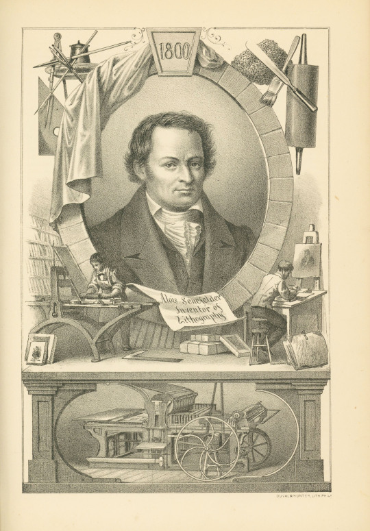

On this day, November 6, 1771, Alois Senefelder (1771-1834) inventor of lithography was born. The son of an actor and tasked with supporting his mother and siblings after his father’s death, Senefelder began his own acting career at age twenty and extended his occupational talents into playwriting. Unable to afford to publish a new play he’d written, Senefelder experimented with what he called “stone printing” in the 1790s, etching acid resistant ink onto limestone and subsequently inventing the first planographic process in printing. Senefelder perfected the chemical process and designed a special printing press with the help of the André family and within five years lithography was being used as a cheap form of creating reproductions by publishers and in mapmaking by land surveying offices throughout Europe.
By the early 1800’s Senefelder and his contemporaries were thinking of ways to introduce color to lithography. Senefelder outlined his ideas on chromolithography in his 1818 book A Complete Course of Lithography, but it was Godefroy Engelmann of France who was awarded the patent for it in 1837.
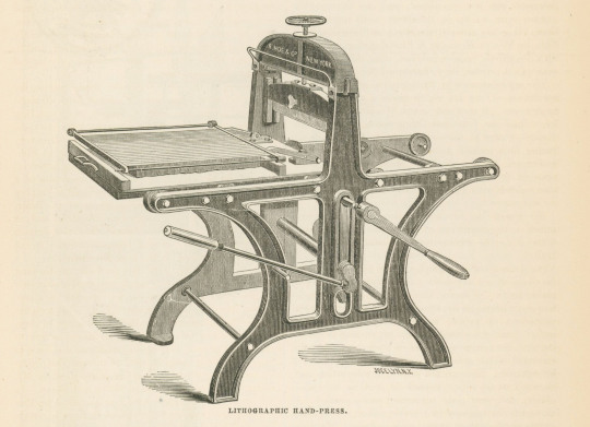
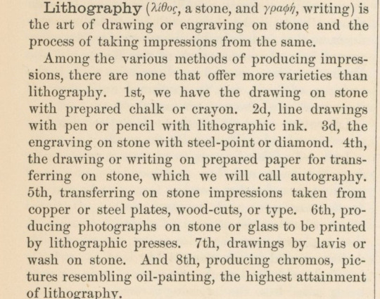
In celebration of Senefelder’s birthday and all that he contributed to the printing world; we’re looking at the American Encyclopedia of Printing published in 1871 by Menamin & Ringwalt of Philadelphia. Included within the section on lithography is a storied portrait of Senefelder surrounded by his tools and accomplishments. The lithographic portrait was printed by Duval & Hunter, lithographers and chromo publishers out of Philadelphia.
It wasn’t long before artists saw the appeal of lithographs and began taking advantage of the new printing technique. Lithography was far more approachable than other printing methods of the time like engraving, because artists could draw directly on the stone with familiar tools, such as pens and crayons. They did not need to master a new medium or skill to create highly accurate prints with deep textural qualities.
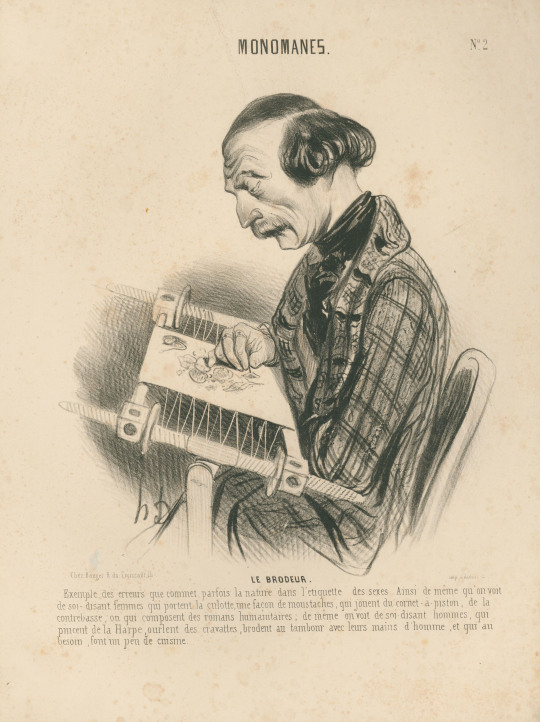
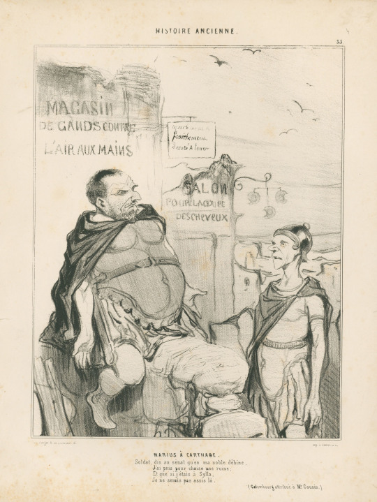
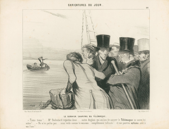
Among the artists of the 1800’s diving into lithography, Honoré-Victorin Daumier (1808-1879) excelled in the medium. Daumier was a prolific French artist who created more than 4,000 lithographs in addition to his many sculptures, paintings, drawings, and wood engravings. His specialty was satirical social caricatures of Parisian life where he effortlessly blended artistry, social commentary, and humor as showcased in the following lithographs held within our collection. The prints were published in 1840 by La maison Aubert of Paris.


View other posts from the American Encyclopedia of Printing.
View more posts with lithographs.
View more Milestone Monday posts.
– Jenna, Special Collections Graduate Intern
#Milestone Monday#milestones#alois senefelder#lithography#planographic printing#J. Luther Ringwalt#American Encyclopedia of Printing#Menamin & Ringwalt\#Duval & Hunter#Honoré-Victorin Daumier#Daumier#La maison Aubert#lithographs#inventions
18 notes
·
View notes
Note
hey, quick question because i'm not sure what to search online to find it and iirc you did/do metalworking etc so i thought i'd ask: what's the term for when you emboss metal but then darken the surroundings so the embossed designs contrast/'pop' more?
I'm not sure there's one particular term for the two processes you're describing, but I could be wrong! 'Patination/patinating' is the word that comes to mind: the creation of an oxide layer on the metal to create a different colour. It's only surface deep, and can usually be polished or sanded off, depending on how thick the layer is. It's a separate process from embossing.
Embossing (chasing and repoussé) is pretty much just the moving of metal into a raised pattern or relief, and you can either bring out the details with an oxidising fluid/antiquing fluid or leave it as it is. Metals are usually oxidised with acids to produce a darker surface finish, which is often then polished away from the high points to create contrast. With silver or copper (though not brass), you generally use liver of sulphur, and with ferrous metals often a selenious acid is used in commercial 'antiquing fluids', but there are a number of others that work. You can also use heat to produce different oxides and colours on the surface, but you have to be careful about affecting the temper/hardness of steel, and know that any other metals or materials will be affected differently with heat.
This is an interesting article from the Met about techniques of metalwork decoration.
Other methods related to this are: gilding, damascening (mechanical rather than chemical application of a softer metal (gold) to a harder one (steel)), blueing (chemical or hot, but it's still a patina, specifically for ferrous), chemical etching (vs mechanical engraving).
This amazing 16th century armour from the Wallace Collection has all of the above:

I'm not sure I've really answered your question, so feel free to drop back with more if I can help any further!
15 notes
·
View notes
Photo
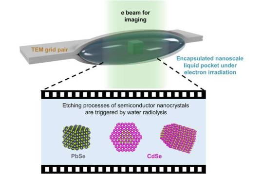
Liquid cell transmission electron microscopy analysis of semiconductor nanocrystals
Semiconductor nanocrystals of different sizes and shapes can govern the optical and electrical properties of materials. Liquid cell transmission electron microscopy (LCTEM) is an emerging method to observe nanoscale chemical transformations and inform the precise synthesis of nanostructures with expected structural features. Researchers are investigating the reactions of semiconductor nanocrystals with the method to study the highly reactive environment produced via liquid radiolysis during the process.
In a new report now published in Science Advances, Cheng Yan and a research team in Chemistry and Materials Science at the University of California Berkeley, and the Leibniz Institute of Surface Engineering, Germany, harnessed the radiolysis process to replace the single particle etching trajectory of prototypical semiconductor nanomaterials. Lead selenide nanotubes used during the work represented an isotropic structure to retain the cubic shape for etching through a layer-by-layer mechanism. The anisotropic arrow-shaped cadmium selenide nanorods maintained polar facets with cadmium or selenium atoms. The trajectories of transmission liquid cell electron microscopy revealed how the reactivity of specific facets in liquid environments governed the nanoscale shape transformations of semiconductors.
Read more.
#Materials Science#Science#Transmission electron microscopy#Semiconductors#Nanocrystals#Materials Characterization#Liquids
11 notes
·
View notes
Text
Factors That Affect the Cost of Engraving and chemical etching

Engraving and chemical etching are techniques used to create designs or patterns on various materials, including metal, glass, and plastic. Engraving involves using a tool or machine to physically cut or remove material from the object's surface, creating a recessed or raised design. On the other hand, chemical etching uses a chemical solution to dissolve or etch away the material. You can recess into the surface by creating a layout. Both techniques create intricate designs and patterns.
However, the cost of these processes can vary greatly depending on several factors. This post will examine several essential elements that impact engraving and chemical etching costs.
Type of Material
One critical element affecting these operations' price is the type of metal being etched or engraved. Some metals, such as stainless steel, are more expensive than others. This will be reflected in the price of the final product. Additionally, the thickness of the metal can also affect the cost, as thicker materials may require more time and resources to etch or engrave.
Design Complexity
The complexity of the design is another factor that can affect the cost of engraving and chemical etching. More complex procedures like custom signs may require more time and resources to produce. Also, designs requiring multiple colours or layers may affect the price.
Customization
Customization is another factor that can affect the cost of engraving and chemical etching. Suppose a customer requests modifications or changes to the design or engraved sign. These requests can add additional time and resources to the process. Additionally, if a customer requests unique things like custom signs or special materials, this can also affect the cost of the process.
Quantity
The quantity of parts produced is another factor affecting the cost of engraving and chemical etching. Due to economies of scale, the cost per part will usually decrease as the quantity increases. However, it's important to remember that extremely large quantities may require additional resources and setup time which can increase the final cost.
Additional Services:
Additional services can also affect the cost of engraving or etching. For example, if you require different finishing or polishing on the engraved signs or etched pieces, this can add to the price. Similarly, if you need to ship the item to a specific location, this can also add to the cost.
Many companies provide chemical etching services for the production of high-precision metal parts. With over two decades of expertise, they are known for producing delicate and intricate details as fine as 0.35mm.
How to find the correct service provider:
Research different chemical etching companies: Look for companies with experience in the type of etching you require. Check for customer reviews to gauge their reliability and quality of work.
Consider the service provider's capabilities: Confirm that the company can produce parts with the level of precision and complexity that you require.
Assess the lead time and cost: Many companies provide cheap engraving services. Compare different providers' lead time and cost to ensure you get a cost-effective and timely service.
Check for additional services: Find out if the company offers other services, such as multi-colour fills, to ensure that you have a one-stop shop for all your etching needs.
Please communicate with the service provider: Reach out to the company and ask any questions to ensure they are the right fit for your project.
Final Thoughts
Several factors can affect the cost of engraving and chemical etching. Many service providers provide cheap engraving services, but it is essential to remember that the most affordable option may only sometimes offer the best quality or meet your specific needs.
However, chemical etching and engraving are cost-effective and efficient methods of producing high-quality and precise metal parts despite these factors.
2 notes
·
View notes
Text
Clean Way to Remove Impurities - Abrasive Water Blasting
Abrasive water blasting is a technique that has been in play since 1870. This technique uses water and soap to enable degreasing with a synchronous blasting to eliminate dust and hazardous material or waste(asbestos or other impurities). It doesn’t pose any danger to surfaces and structures, resulting in effective decontamination. This is done by Abrasive Water Blasting Equipment which varies in size and pressure.
Abrasive water blasting forcibly propels abrasive material against a surface under high pressure to achieve the following:
● Smoothing of a rough surface
● Roughening of a smooth surface
● Shaping of a surface
● Removal of surface contaminants
The Aqua Miser’s abrasive water blasting process can be done using all traditional blasting formats such as walk-in booths, hand cabinets, automated production machinery, and total loss portable blasting units. The speed of the process depends upon the requirement. The surface which has been cleaned using the process is not damaged as water acts as a buffer. Thus, there are two advantages of abrasive water blasting, it decreases media breakdown rate, and second, it prevents foreign material from sticking to the surface. The level of cleanliness of water blasting is way better than dry blasting because of which it is preferred before coating or bonding operations too.
Types of Wet Blasting Techniques
There are several wet blasting techniques presently available for the choice. Few of them are
● Wet Abrasive Blasting
● High-pressure water blasting
● High-pressure water and abrasive blasting
● Air and water abrasive blasting
The choice of blasting method depends upon the requirement and according to the application.
Abrasive Water Blasting Equipment Details
The wet blast devices are mostly of cabinet-mounted type that can be easily modified. You can take-off conveyors, auxiliary strippers, and wash-rinse dry stations. The blasted device is usually composed of the following parts:
● Vertical wheel
● Horizontal plane turntable
● Shuttle with rail/car extensions
● Chain/belt conveyors
● Self-contained turning mechanisms for shafts and tubular parts
● Combination of tumbling-cabinet machines.
How Does Abrasive Blasting Work?
Abrasive water blasting equipment involves the propulsion of a slurry towards a surface with the help of a high-velocity air propulsion system. The slurry is finely abrasive mixed in chemically treated water. involves high-velocity compressed air propulsion of a slurry towards a surface. The compressed air is sent into a vessel at a pressure equal to that fed to a blast hose. The pressure is equalized to enable the abrasive mixture to feed into an airline. A full flow valve is located between a hopper and mixing chamber which is used to control the flow of abrasives.
Applications of Wet Abrasive Blasting
The applications of wet abrasive blasting are as follows:
● Burr removal from substrates
● Preparation of surface for hard chrome coatings, bonding composites, bonding coatings, bonding composites, and tine and other tool coatings.
● Aviation engine rebuilding
● Etch glass for decorative or functional purposes
● Peen surfaces for a bright, and clean appearance
● Automotive overhaul and engine rebuilding
● Clean plastic injection molds
● Hole cleaning for printed circuit boards
Benefits of Wet Abrasive Blasting
The list of benefits of abrasive blasting is long but key benefits of wet abrasive blasting are listed below:
● Extremely fine media can be used
● Media impregnation into the substrate is not possible
● Deeply cleans irregular surfaces
● Eliminates the need for hand-sanding
● Eliminates the need to use toxic chemicals
● Reduces dust
● Closed cabinet recycles media/slurry
● No heat warping with thin parts
● Final finish is appealing with a satin feel
● Provides an excellent surface for plating
● Provides an excellent surface for bonding
● Holds tight tolerances
5 notes
·
View notes
Text
How Laser Engraving Machines Revolutionized Metal Marking?

The field of metal marking has undergone significant transformation over the years, primarily due to advancements in technology. Among these advancements, the introduction and development of laser engraving machines have played a pivotal role.
Engraving machine lasers have revolutionized the way industries mark metal, offering unparalleled precision, efficiency, and versatility. This article explores how these machines have changed metal marking machines and the benefits they bring to various industries.
The Evolution of Metal Marking Machine
Traditionally, metal marking machines involved methods such as stamping, etching, and engraving. While effective, these methods often had limitations in terms of precision, speed, and flexibility. Stamping, for instance, could deform the metal, while chemical etching poses environmental and health risks.
The advent of laser technology addressed many of these issues, providing a cleaner, more precise alternative.
The Mechanics of Laser Engraving
Laser engraving machines utilize focused beams of light to etch designs, serial numbers, barcodes, and other identifiers onto metal surfaces. This process involves the following steps:
Generation of Laser Beam: The machine generates a high-intensity laser beam, which is directed towards the metal surface.
Focusing the Beam: The laser beam is focused onto a small area of the metal, where the intense energy causes the surface to vaporize or oxidize, leaving a permanent mark.
Controlled Movement: Advanced software controls the movement of the laser, allowing for intricate designs and precise markings.
This method offers several advantages over traditional marking methods, making it the preferred choice for many industries.
Advantages of Laser Engraving Machines
Precision and Detail
Laser engraving machines provide exceptional precision, capable of producing detailed and intricate designs. This level of accuracy is essential for industries requiring high-quality marks, such as aerospace, automotive, and electronics.
Speed and Efficiency
These machines operate at high speeds, significantly reducing the time required for marking processes. This efficiency allows manufacturers to increase production rates without compromising on quality.
Versatility
Laser engraving machines can mark a wide variety of metals, including stainless steel, aluminium, brass, and titanium. Because of their adaptability, they are appropriate for a wide range of applications in various sectors.
Non-Contact Process
Unlike traditional methods that may physically impact the metal, laser engraving is a non-contact process. This reduces the risk of damage or deformation to the metal, ensuring the integrity of the components.
Durability and Permanence
Marks created by laser engraving are highly durable and resistant to wear, chemicals, and high temperatures. This durability is crucial for parts exposed to harsh environments.
Eco-Friendly
Laser engraving is an environmentally friendly process as it eliminates the need for chemicals and produces minimal waste. This aligns with the growing emphasis on sustainable manufacturing practices.
Applications of Laser Engraving Machines
Manufacturing:
In manufacturing, laser engraving machines are used to mark parts with serial numbers, barcodes, and logos. This helps in tracking and quality control, ensuring that each part can be traced throughout the production process and beyond.
Aerospace:
The aerospace industry relies on laser engraving for marking critical components with detailed specifications and identification marks. The precision of laser marking ensures compliance with stringent regulatory standards.
Medical Devices:
Medical devices require precise and permanent markings for identification and compliance purposes. Laser engraving is ideal for this application, providing high-resolution marks on surgical instruments, implants, and equipment.
Jewelry and Personalization:
Laser engraving is widely used in the jewelry industry for creating intricate designs and personalizing items with names, dates, and messages. The precision and fine detail achievable with laser engraving enhance the value and appeal of these products.
Conclusion
Laser engraving machines have undeniably revolutionized metal marking machines, offering superior precision, efficiency, and versatility. By addressing the limitations of traditional marking methods, these machines have become indispensable tools in various industries.
The benefits they bring, from eco-friendliness to enhanced durability of marks, make them a critical component in modern manufacturing and production processes. As technology continues to advance, we can expect further innovations in laser engraving, continuing to transform the landscape of metal marking machines.
0 notes
Text
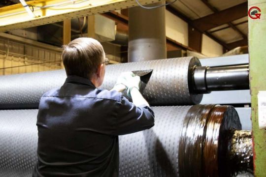
Exploring The Craftsmanship Of Engraved Cylinders And Rubber Rolls
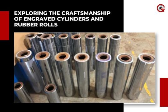
(Source – IndiaMart)
Engraved cylinders and rubber rolls are indispensable components in various industrial processes, playing critical roles in printing, embossing, laminating, and more. Despite their understated presence, these precision-engineered tools demonstrate the convergence of craftsmanship, engineering, and innovation. In this article, we delve into the intricacies of engraved cylinders and rubber rolls, their manufacturing processes, applications across industries, and the advancements shaping their future.
Understanding Engraved Cylinders and Rubber Rolls:
Engraved cylinders, also known as gravure cylinders or printing cylinders, serve as the backbone of gravure printing, a high-quality and high-speed printing process widely used in packaging, publishing, decorative printing, and security printing. These cylinders are meticulously engraved with recessed cells or dots, each representing a specific color or image detail. The depth, shape, and arrangement of these cells determine the ink-carrying capacity and printing precision.
The Manufacturing Process:
https://gqresearch.com/wp-content/uploads/2024/05/2.2-_-The-Manufacturing-Process_-Source-Inbound-Logistics.jpg
The production of engraved cylinders is a blend of artistry and precision engineering. Initially, the cylinder surface, typically made of copper or chrome-plated steel, undergoes meticulous polishing to achieve a flawless finish. Subsequently, skilled artisans employ various engraving techniques, including electromechanical engraving, laser engraving, and chemical etching, to create the desired patterns or images on the cylinder surface. Each method offers unique advantages in terms of speed, precision, and suitability for different materials.
Electromechanical engraving involves using a diamond-tipped stylus to directly carve the design onto the cylinder’s surface. Laser engraving, on the other hand, utilizes high-energy laser beams to vaporize or ablate the cylinder material, offering exceptional precision and versatility. Chemical etching involves coating the cylinder with a photosensitive resist, exposing it to ultraviolet light through a mask containing the desired pattern, and then chemically etching away the unexposed areas to create the engraved design.
Applications Across Industries:
Engraved Cylinders and Rubber Rolls find widespread application in various industries, including flexible packaging, label printing, wallpaper manufacturing, and currency printing. In flexible packaging, gravure printing delivers vibrant colors and intricate designs, enhancing product appeal and brand recognition. Label printing utilizes engraved cylinders to achieve precise graphics and text, catering to diverse labeling requirements in food, beverage, pharmaceuticals, and cosmetics.
Moreover, engraved cylinders play a pivotal role in specialty printing applications, such as security printing and decorative laminates. In security printing, intricate patterns, micro-text, and holographic elements engraved on cylinders deter counterfeiting and ensure document authenticity. Decorative laminates, used in furniture, flooring, and interior design, feature embossed textures and patterns created through engraved cylinders, adding aesthetic value and tactile appeal.
Engraved Cylinders and Rubber Rolls: The Unsung Heroes of Industrial Processes
While Engraved Cylinders and Rubber Rolls take the spotlight in printing and embossing, rubber rolls quietly support a myriad of industrial processes, including web handling, laminating, coating, and embossing. These versatile components, typically made of synthetic rubber or elastomers, exhibit exceptional resilience, durability, and surface uniformity, making them ideal for conveying, spreading, or compressing materials in diverse manufacturing environments.
Manufacturing Rubber Rolls:
The manufacturing process of rubber rolls involves precision engineering and specialized rubber compounding techniques to achieve the desired mechanical properties and surface characteristics. Initially, raw rubber compounds, comprising elastomers, fillers, plasticizers, and curing agents, are mixed and processed to form uniform sheets or strips. Subsequently, these sheets undergo precision machining, grinding, or molding to produce the final rubber roll components.
The surface finish and hardness of rubber rolls are critical parameters determined by the application requirements. Hard rubber rolls, characterized by high durometer values, offer superior wear resistance and dimensional stability, making them suitable for heavy-duty applications such as calendering and embossing. In contrast, softer rubber rolls provide enhanced grip and cushioning, ideal for applications requiring gentle material handling or delicate surface treatment.
Diverse Applications and Advancements:
Engraved Cylinders and Rubber rolls find extensive use across industries, serving as essential components in printing presses, laminators, embossing machines, and converting equipment. In printing applications, rubber rolls facilitate precise ink transfer and web tension control, ensuring consistent print quality and registration accuracy. In laminating processes, rubber rolls apply uniform pressure to bond adhesive layers and substrates, producing durable composite materials.
Recent advancements in material science and manufacturing technology have further expanded the capabilities of rubber rolls, enabling customization of surface properties, such as coefficient of friction, release characteristics, and anti-static properties, to meet specific application requirements. Additionally, innovations in roll coating technologies, such as laser-engraved coating patterns and nanostructured surfaces, have enhanced coating uniformity and efficiency, enabling precise control over coating thickness and distribution.
Conclusion:
Engraved cylinders and rubber rolls exemplify the marriage of craftsmanship, engineering, and innovation in industrial manufacturing. From precision engraving techniques to specialized rubber compounding, these components play indispensable roles across diverse industries, driving efficiency, quality, and innovation. As advancements continue to shape the landscape of industrial processes, engraved cylinders and rubber rolls remain steadfast pillars of modern manufacturing, underscoring their enduring relevance and significance in the ever-evolving industrial ecosystem.
#IndustrialManufacturing#Craftsmanship#EngineeringInnovation#IndustrialApplications#InnovativeTechnolog
0 notes
Text
Introduction to Audio Amplifier PCBs

The initial section would set the stage by outlining the critical role of PCBs in audio amplification, emphasizing their impact on sound quality and system reliability. It would introduce the reader to the basic types of audio amplifier PCBs, such as Class A, Class B, Class AB, and Class D, each offering distinct advantages and suited for different applications.
Detailed Analysis of PCB Components and Design
A thorough exploration of the components that make up an audio amplifier PCB would follow. This would include an in-depth look at resistors, capacitors, inductors, and the various semiconductor devices such as transistors and integrated circuits. The discussion would extend to design considerations like PCB layout, signal integrity, noise reduction, and thermal management, crucial for optimizing performance and durability.
Material Science and Innovation
This section would delve into the materials used in PCB construction, comparing traditional materials like FR4 with more advanced options like metal-core boards, particularly focusing on their thermal conductivity and durability under high-power conditions. Innovations such as flexible PCBs for more compact and versatile designs would also be highlighted.
Manufacturing Processes and Quality Assurance
The manufacturing process for audio amplifier PCBs would be examined, from etching and drilling to plating and final assembly. Quality assurance processes, including testing methods like Automated Optical Inspection (AOI), In-Circuit Testing (ICT), and functional testing, would be detailed to emphasize their importance in ensuring product reliability.
Applications and Case Studies
Real-world applications of audio amplifier PCBs in various industries would be presented. This would include their use in consumer electronics, automotive audio systems, professional audio equipment, and even in military applications. Case studies from leading manufacturers and designers would illustrate how innovative PCB design has solved specific audio challenges or enhanced performance.
Regulatory and Environmental Considerations
Compliance with international standards such as the IPC (Institute for Printed Circuits) standards, and environmental regulations like RoHS (Restriction of Hazardous Substances) and REACH (Registration, Evaluation, Authorization, and Restriction of Chemicals) would be covered. This section would discuss how these regulations impact the design and disposal of audio amplifier PCBs and what steps manufacturers are taking to reduce environmental impact.
The Future of Audio Amplifier PCBs
Exploring future trends and technologies, this section would speculate on the advancements in PCB design and materials, such as the integration of AI for smart diagnostics and the use of graphene and other nanomaterials for enhanced performance. It would also consider the impact of emerging markets and technologies on the demand and design of audio amplifier PCBs.
Conclusion
The final part of the guide would summarize the critical points discussed, reinforcing the importance of innovative, well-designed audio amplifier PCBs in the advancement of audio technology. It would also encourage ongoing research and development efforts within the field to meet the evolving demands of the industry.
This extensive guide would not only serve as an educational tool but also as a reference for designing next-generation audio amplifier PCBs, combining theoretical knowledge with practical insights to push the boundaries of audio technology.
0 notes
Text
WHAT IS BETTER 18K OR 24K FOR GOLD PLATING JEWELRY DESIGN?
To gold plate something, you put a tiny layer of gold on top of a base metal. Making a lot of different kinds of gold-plated jewelry design involves this step.
The jewelry can really look like solid gold. This type of jewelry design, on the other hand, is much less expensive. Because of this, gold finishing is very common for both cheap and expensive jewelry.
There are differences in how thick and good the gold covering is. Because of this, you need to know about gold covering before you buy. On top of that, gold layering does fade over time. So, you need to take good care of gold jewelry design to make sure it lasts a long time. So be careful, especially if you use it more often. In general, though, gold finishing is an excellent method to get the fancy look of gold by not spending a lot of money.

WHAT 18K AND 24-K GOLD PLATING MEAN?
To comprehend how gold stacking works, you need to know a few things about gold. Karats (k) are a way to measure gold. 24k is the purest form of gold. To make jewelry design, though, pure gold tends to be soft. People often blend it with metallic substances to make it stronger. This is where 18k gold plating as well as 24k gold plating vary.
75% of 18-k gold is pure gold as well as 25% is different metals. The 24-k gold lining, on the other hand, is a coat of real gold. Electroplating on an initial metal made it possible for it to exist. It is more sturdy and more resistant to discolor than 24-k gold, but 24-k gold plating looks more expensive and rich. Which type of gold plating to use relies on the jewelry design’s style and purpose.
18-K and 24-K gold plating are mixed together
When it comes to gold layering from Indian jewelry online, most people use two designs. Some of them are 18-karat and 24-karat. The amount of gold within each is the main difference among them. 24-karat gold enamel is 100% pure gold, while 18-karat gold enamel has 75% gold in it. Electroplating, also a thin layer of gold into a base metal is what it does. That’s why both kinds of gold enamel utilize either etching or electroless treatment.
When you electroplate, you run an electric current with a solution that has gold ions in it. Electroless layering, on the other hand, uses a chemical process. An artificial mix of gold ions as well as the metal are reacting without electricity. Both ways result in effective, even, deep plating that gives different finishes for different uses.
18-K and 24-K gold plating are not all the same color
You can tell the distinction in color between 18-k and 24-k gold finishing in Indian jewelry online, particularly when it comes to rose and white gold. When making 18-karat gold, though, people often mix it with different metals like copper, silver, and zinc. Because of this, the gold looks more yellow rather than as vibrant as 24-k gold. On another hand, 24-k gold is pure gold. The procedure also changes the metal’s surface, leaving it more malleable and simple to scratch while also making it look lighter.
The best way to get a rose gold polish is to use 18-k gold treatment. Because it has copper in it, 18-k has a red color. For a white gold look, though, 24-k gold works best because it has a tone more like silver. In the end, the choice within 18-k and 24-k gold finishing comes down to your own preferences and how you want your jewelry to look.
18-K and 24-K gold plating cost different amounts
It is important to know the difference between 18-k and 24-k gold if you are thinking about gold plating. Gold that is 18-k is 75% gold and 25% additional metals. Gold that is 24-k is 99.9% gold. It indicates that 24-k gold enamel costs more and has greater amounts of gold in it than 18-k gold plating. The disparity in cost among the two can be very big or very small, based on the project. A 24-karat gold covering is still usually a high-end choice for things like jewelry or high-end electronics.
You could opt for 18-k gold layers, though, if you want something that will be useful a lot of the time. It lasts longer and doesn’t fade as easily. Before you choose one of these choices, you should know what you need to know regarding gold and the way it affects the price difference between plating types.
How long 18-K and 24-K gold plating lasts and how well it wears?
When it comes to gold plating, longevity and durability are very important things to think about. For instance, 18-k and 24-k gold-plated items last longer and are more durable than lower-karat choices. You can choose between 14k gold or 10k gold. But even this much gold plating may rub off over time, mostly if it is not treated properly. You should keep gold-plated jewelry away from strong chemicals or rough surfaces because of this. Also, don’t wear it when you swim or take a shower.
Polishing and cleaning gold-plated jewelry on a regular basis will also keep it looking good and make it last longer. The gold finish will wear off over time, though, even with good care, showing the base metal below. If you want 18-k or 24-k gold plating to last longer, you need to take good care of it and keep it in good shape.
Normal uses for 18-K and 24-K gold plating
Gold is a popular metal for Indian jewelry online makers because it is smooth and simple to scratch or damage. Jewelry often uses 18 karat (18k) gold finishing, which is 75% pure gold. It’s a good mix of longevity and value for money. Such a good material for everyday use makes it perfect for engagement rings, bracelets, as well as chains.
24k gold plating, contrary to popular belief, is made of 99.9% pure gold as well as the best gold which can be used to make jewelry. It makes the jewelry piece look more expensive and shiny. Luxury items like watches, buttons, and earrings often use 24 karat gold. However, because it is soft, there are choices that last longer, and it needs more care to keep its shine.
People often put 18-k enamel on Indian jewelry online, gadgets, and car parts to make them look nice. People use 24-k metal for both surgical posts and high-end expensive items at the same time. Both types of enamel are useful in their own ways, but 24-k gold plating is usually more expensive. It’s because there is a lot of pure gold in it. Even so, 18-k is still popular because it lasts a long time and can look like more expensive things.
Conclusion
This change in purity in jewelry means that the price is also different. For instance, pure 24k gold costs more than 18k gold because it has more gold in it. Gold plating is a good idea because it makes the thing more valuable and lasts longer. What makes the cost distinct among them both in the end relies on two things. They say how big the thing is that needs coating and how much gold it needs. Because of this, it is important to talk to a professional you can trust before choosing which gold plating plan to go with.
Courtesy: Poojamani Jewellers
0 notes
Text
Enhancing Semiconductor Manufacturing: Nitrogen Generator Essentials
Modern life is increasingly reliant on the power and versatility of semiconductors. From smartphones and laptops to the complex circuitry behind medical equipment and self-driving cars, these tiny chips are the driving force of technological innovation. Their intricate production process relies on a variety of vital components, one of which is a reliable and efficient Nitrogen Generator.
The Role of Nitrogen in Semiconductor Manufacturing:
Nitrogen, the most abundant gas in Earth’s atmosphere, plays a critical role in several stages of Semiconductors manufacturing. Here’s an explanation of its main uses:
Inert Atmosphere Creation: Pure nitrogen (up to 99.9995%) acts as an inert gas, preventing oxidation and contamination during critical steps like photolithography, etching, and deposition. This is crucial because even slight impurities can significantly impact the electrical properties and functionality of the finished chip.
Plasma Cleaning: During the cleaning process, nitrogen plasma removes organic contaminants, photoresist residues, and other unwanted substances from the wafer surface.
Sputtering: In this technique used for depositing thin films onto the wafer, nitrogen is often combined with other elements to create specific material properties.
Nitrogen: An Inert Ally in the Semiconductor World
Nitrogen plays a crucial role in the complex world of Semiconductor manufacturing. Its most significant contribution lies in its inherent property – inertness. Unlike oxygen, which readily reacts with other elements, nitrogen remains stable, making it ideal for various stages of the process.
One key function is purging. By flowing nitrogen gas through equipment and over surfaces, it displaces oxygen and other contaminants like water vapor and particles. This creates a clean and controlled environment, preventing unwanted chemical reactions that could damage the delicate circuitry being etched onto the semiconductor wafers.
Also Read: – Sustainable operations the role of PSA technology in nitrogen Generation
Types of Nitrogen Generators
Two primary types of nitrogen generators are widely used in semiconductor manufacturing:
Pressure Swing Adsorption (PSA): This technology utilizes zeolite beds to selectively adsorb other gases from compressed air, leaving behind purified nitrogen. PSA generators are known for their energy efficiency and are suitable for applications requiring moderate purity levels.
Membrane Separation: This method employs specialized membranes that selectively allow nitrogen molecules to pass through, separating them from other gases in the air. Membrane generators are ideal for producing high-purity nitrogen and offer compact footprints.
Choosing the Right Nitrogen Generator
Selecting the optimal Nitrogen Generator for your specific needs is crucial for ensuring the smooth operation and efficiency of your semiconductor manufacturing process. Here are some crucial factors to consider.
Purity: – The level of nitrogen purity required will vary depending on the specific application. For critical processes like photolithography, ultra-high purity nitrogen (UHP) with impurity levels below 1 ppm is necessary.
Flow Rate: – The required nitrogen flow rate depends on the volume of your cleanroom and the specific processes conducted. Generators can deliver a range of flow rates, from low volumes for research labs to high volumes for large-scale production facilities.
Reliability and Uptime: – Uninterrupted nitrogen supply is essential to maintain consistent production and prevent costly downtime for generators known for their reliability and low maintenance requirements.
Cost-Effectiveness: – While initial cost is important, consider the long-term efficiency and operating costs of the generator. Factors like energy consumption and maintenance costs should be factored into the decision.
Conclusion:
A reliable and efficient nitrogen generator is critical for ensuring the smooth operation and high-quality production in semiconductor manufacturing. By understanding the role of nitrogen, its various applications, and the key factors to consider when choosing a generator, you can optimize your production process and lay the foundation for success in this ever-evolving field. Remember, choosing the right nitrogen generator is a crucial investment in the quality, efficiency, and ultimately, the success of your semiconductor manufacturing operation.
0 notes
Text
Revolutionizing Car Care: The Deionized Water Filter Car Wash
In the world of automotive enthusiasts and detailers, the quest for the perfect car wash solution is akin to an alchemist seeking the philosopher's stone. The emergence of deionized water filter car wash systems has brought us one step closer to that elusive ideal. In this article, we'll delve into what makes these systems so revolutionary and why they're becoming a game-changer for car owners and professionals alike.

What is Deionized Water?
Deionized water is essentially water that has had its mineral ions removed. This purification process involves passing water through ion exchange resins or other specialized filtration methods, resulting in water that is nearly free of impurities. Unlike tap water or even distilled water, which may still contain trace minerals and impurities, deionized water is exceptionally pure.
The Science Behind Deionized Water Car Washes
The magic of deionized water lies in its purity. When used for washing cars, it leaves behind no mineral deposits or water spots. Traditional car washes often rely on tap water, which contains minerals like calcium and magnesium. When this water evaporates, it can leave behind unsightly spots and streaks on the vehicle's surface. Deionized water eliminates this problem entirely, leaving a spot-free, streak-free shine.
Moreover, since deionized water is free of impurities, it's also a safer option for sensitive automotive surfaces like paint, chrome, and glass. It reduces the risk of scratching or etching that can occur when washing with hard water.
The Deionized Water Filter Car Wash System
So, how does one go about incorporating deionized water into a car wash? This is where the deionized water filter car wash system comes into play. These systems typically consist of a series of filtration stages designed to remove minerals and impurities from the water supply.
The process begins with water entering the filtration system, where it passes through various stages of filtration, including sediment filters, carbon filters, and finally, deionization resin cartridges. These resin cartridges are the heart of the system, effectively removing any remaining ions from the water, leaving it pure and deionized.
Once the water has been filtered and deionized, it's ready to be used for washing vehicles. Whether through a traditional hose and bucket method or a specialized pressure washing system, deionized water ensures a clean, streak-free finish every time.
Benefits of Deionized Water Car Washes
The benefits of using a deionized water filter car wash system are numerous:
Spot-Free Shine: Deionized water eliminates the risk of water spots and streaks, leaving vehicles with a flawless finish.
Protection for Automotive Surfaces: By reducing the risk of scratching and etching, deionized water helps preserve the integrity of paint, chrome, and other sensitive surfaces.
Environmental Friendliness: Since deionized water doesn't contain harsh chemicals or additives, it's an environmentally friendly option for car washing.
Time and Cost Savings: With no need for drying or buffing to remove water spots, Cr Deionized Water System can save time and money for both enthusiasts and professionals.
0 notes
Text
Laser Engraving And Laser Marking Similar Or Different Processes?
Laser etching, marking, and engraving are the most versatile modern inventions that are used in almost every industrial sector. While the difference between the laser engraving and laser marking and laser etching is quite evident, the terms laser marking and engraving are confused at times. Laser marking, is a method that leaves markings on a surface material of an object, including colour change, owing to chemical alteration.
Laser engraving is the method that is carried out by inscribing on an object surface. Laser engraving does not involve any inks or dyes, so it gains an advantage over the laser marking, wherein the replacement of tool bits like the ink heads need not be done. Laser marking has its own pros like the preservation of surface without any impact on it, since it uses colours and dyes to mark on the material surface thorough the laser techniques. Laser-sensitive polymers, metal alloys play an important role in this method. The method in general is a generic term that encompasses a variety of surfacing marking techniques like printing, hot-branding, laser attachment and so on.
On the other hand Laser engraving selectively removes minute layers of the surface material creating visibly conspicuous marks which are permanent. Different material surfaces respond to the laser in different ways. Harder surfaces primarily are responsive to ablation where the laser beam dislodges the minute particles from the surface. Engraver can create deep incisions, whereas laser marking is usually much shallower comparatively. Very short bursts of precise laser pulses or beams are done to get a clear marking, as transmit large quantity of power even without high degree of heating or melting the material surface.
Laser engraving is a part or a subsection of laser marking but however since it differs in quite a few ways it is separated from the laser marking. Mainly there are three types or categories in laser engraving, Laser ablation, deep laser engraving and laser etching. The difference in these three is the amount or the depth of engraving that is carried out depending on the requirement and the nature of the material surface. Laser ablation is the quickest way to mark on a material surface. This method is most suitable for engraving on parts that are subjected to high wear, marking serial numbers; logos, engine and chassis number engraving and so on. In laser etching, engraving is carried by the heat caused by the beam on to the surface of the material.
Nevertheless machines that are used for laser engraving and laser marking are almost similar, by virtue of the technology. But in a lot of cases these terms are confused due to the lack of awareness. Organizations like Signvec are pioneers in supply and service of laser marking machine and laser engraving machines. Located in Singapore the company has carved out a solid place for itself in the mentioned sector and has been maintaining a solid clientele, with reputed names included in it.
In Order To Find Out More Details On Laser Engraver Please Be Touch With Us Today Onwards..!
#Laser Engraver#Laser Engravers#Laser Engraving Machine#Laser Engraving Machines#Fiber Laser Marker#Fiber Laser Marking Machine#laser marking machines#laser marking machine
0 notes
Text
Exploring the Versatility of Fiber Laser Marking Machines
In today’s fast-paced industrial landscape, efficiency and precision are paramount. Whether you’re in automotive manufacturing, electronics, medical devices, or any other industry, the need for clear, permanent, and high-quality markings on various materials is undeniable. This is where fiber laser marking machines come into play, revolutionizing the way products are labeled, tracked, and identified.
Fiber laser marking machines are a powerful tool in the realm of product identification and traceability. Utilizing cutting-edge laser technology, these machines offer unparalleled precision and versatility in marking a wide range of materials, including metals, plastics, ceramics, and even organic materials like wood.
So, what makes fiber laser marking machines stand out? Let’s delve deeper into their features and applications:
Precision Engineering: Fiber laser marking machines employ focused laser beams to create intricate markings with micron-level precision. This level of accuracy ensures that even the smallest details can be marked clearly and consistently, meeting the most stringent quality standards.
Speed and Efficiency: With high-speed scanning systems, fiber laser marking machines can complete marking tasks swiftly and efficiently. This is crucial for industries with high-volume production lines where rapid throughput is essential to meet demand without compromising on quality.
Non-contact Process: Unlike traditional marking methods such as engraving or stamping, laser marking is a non-contact process. This means there’s no physical contact with the material being marked, minimizing the risk of damage or deformation, particularly on delicate surfaces.
Wide Range of Marking Options: Fiber laser marking machines offer versatility in terms of marking options. Whether it’s engraving, etching, annealing, foaming, or color changing, these machines can accommodate various marking techniques to suit specific application requirements.
Compatibility with Various Materials: From metals like stainless steel, aluminum, and titanium to plastics such as ABS, PVC, and polycarbonate, fiber laser marking machines can mark a diverse range of materials with ease. This versatility makes them indispensable across a multitude of industries.
Permanent and Tamper-proof Markings: Laser markings are highly durable and resistant to wear, corrosion, and fading. This ensures that product identification remains intact throughout the lifecycle of the product, enhancing traceability and counterfeit prevention efforts.
Ease of Integration: Fiber laser marking machines can be seamlessly integrated into existing production lines or automated systems, thanks to their compact design and compatibility with various control interfaces. This facilitates smooth workflow integration without significant disruptions to operations.
Environmental Friendliness: Laser marking is a clean and environmentally friendly process that doesn’t involve the use of inks, solvents, or chemicals. This not only reduces operational costs but also minimizes waste and eliminates the need for costly disposal procedures associated with traditional marking methods.
Applications of fiber laser marking machines span across a wide array of industries:
Automotive: From engine components to chassis parts, laser markings play a crucial role in component identification, tracking, and quality control in the automotive sector.
Electronics: In the electronics industry, laser markings are used for branding, serialization, and traceability of circuit boards, semiconductor chips, and electronic devices.
Medical Devices: Laser markings on medical devices ensure compliance with regulatory requirements, facilitate product authentication, and provide essential information such as lot numbers and expiration dates.
Aerospace: In aerospace applications, laser markings are utilized for part identification, serial numbering, and barcoding on aircraft components, ensuring safety and traceability throughout the supply chain.
Consumer Goods: Laser markings are commonly found on consumer goods such as smartphones, appliances, and packaging, serving both functional and aesthetic purposes.
In conclusion, fiber laser marking machines represent a pinnacle of innovation in the field of product identification and traceability. Their precision, speed, versatility, and environmental friendliness make them indispensable tools across a myriad of industries. As technology continues to evolve, these machines will undoubtedly play an increasingly vital role in streamlining manufacturing processes and ensuring product integrity in the global marketplace.
0 notes
Text
A new world of 2D material is opening up - Technology Org
New Post has been published on https://thedigitalinsider.com/a-new-world-of-2d-material-is-opening-up-technology-org/
A new world of 2D material is opening up - Technology Org
Materials that are incredibly thin, only a few atoms thick, exhibit unique properties that make them appealing for energy storage, catalysis and water purification. Researchers at Linköping University have now developed a method that enables the synthesis of hundreds of new 2D materials. Their study has been published in the journal Science.
In a film that measures only a single millimetre, there can be millions of layers of 2D materials which generates its unique properties. Image credit: Olov Planthaber/Linköping University
Since the discovery of graphene, the field of research in extremely thin materials, so-called 2D materials, has increased exponentially. The reason is that 2D materials have a large surface area in relation to their volume or weight. This gives rise to a range of physical phenomena and distinctive properties, such as good conductivity, high strength or heat resistance, making 2D materials of interest both within fundamental research and applications.
“In a film that’s only a millimetre thin, there can be millions of layers of the material. Between the layers there can be a lot of chemical reactions and thanks to this, 2D materials can be used for energy storage or for generating fuels, for example,” says Johanna Rosén, professor in Materials physics at Linköping University.
Three-step process
The largest family of 2D materials is called MXenes. MXenes are created from a three-dimensional parent material called a MAX phase. It consists of three different elements: M is a transition metal, A is an (A-group) element, and X is carbon or nitrogen. By removing the A element with acids (exfoliation), a two-dimensional material is created. Until now, MXenes has been the only material family created in this way.
The Linköping researchers have introduced a theoretical method for predicting other three-dimensional materials that may be suitable for conversion into 2D materials. They have also proved that the theoretical model is consistent with reality.
To succeed, the researchers used a three-step process. In the first step, they developed a theoretical model to predict which parent materials would be suitable. Using large-scale calculations at the National Supercomputer Centre, the researchers were able to identify 119 promising 3D materials from a database and a selection consisting of 66,643 materials.
From theory to lab
The next step was to try to create the material in the lab.
“Out of 119 possible materials, we studied which ones had the chemical stability required and which materials were the best candidates. First, we had to synthesise the 3D material, which was a challenge in itself. Finally, we had a high-quality sample where we could exfoliate and etch away a specific atom layers using hydrofluoric acid,” says Jie Zhou, assistant professor at the Department of Physics, Chemistry and Biology.
The researchers removed yttrium (Y) from the parent material YRu2Si2, which resulted in the formation of two-dimensional Ru2SixOy.
But to confirm success in the lab, verification is necessary – step three. The researchers used the scanning transmission electron microscope Arwen at Linköping University. It can examine materials and their structures down at the atomic level. In Arwen it is also possible to investigate which atoms a material is made up of using spectroscopy.
“We were able to confirm that our theoretical model worked well, and that the resulting material consisted of the correct atoms. After exfoliation, images of the material resembled the pages of a book. It’s amazing that the theory could be put into practice, thereby expanding the concept of chemical exfoliation to more materials families than MXenes,” says Jonas Björk, associate professor at the division of Materials design.
Endless applications
The researchers’ discovery means that many more 2D materials with unique properties are within reach. These, in turn, can lay the foundation for a plethora of technological applications. The next step for the researchers is to explore more potential precursor materials and scale up the experiments. Johanna Rosén believes that future applications are almost endless.
“In general, 2D materials have shown great potential for an enormous number of applications. You can imagine capturing carbon dioxide or purifying water, for example. Now it’s about scaling up the synthesis and doing it in a sustainable way,” says Johanna Rosén.
The study was funded by the Knut and Alice Wallenberg Foundation, the Wallenberg Initiative Materials Science for Sustainability (WISE), the Göran Gustafsson Foundation for Research in Natural Sciences and Medicine, the Swedish Foundation for Strategic Research, the European Union, the Swedish Research Council and the Swedish Government Strategic Research Area in Materials Science on Advanced Functional Materials, AFM, at Linköping University.
Article: Two-dimensional materials by large-scale computations and chemical exfoliation of layered solids; Jonas Björk, Jie Zhou, Per O. Å. Persson and Johanna Rosen; Science 2024. Published online 15 March 2024. DOI: 10.1126/science.adj6556
Written by Anders Törneholm
Source: Linköping University
You can offer your link to a page which is relevant to the topic of this post.
#2024#2D materials#3d#acids#amazing#applications#Article#atom#atomic#atoms#Biology#book#carbon#Carbon dioxide#catalysis#challenge#chemical#chemical reactions#chemistry#Chemistry & materials science news#Database#Design#electron#energy#energy storage#european union#Featured technology news#Foundation#fuels#Fundamental
0 notes
Text
Etching and Deposition Techniques by Nav Sooch: Key Steps in Semiconductor Fabrication
Semiconductor manufacturing is a complex and intricate process that underpins the modern electronics industry. Central to this process are the techniques of etching and deposition, which play crucial roles in defining the intricate patterns and layers of semiconductor devices. From creating nanoscale features to depositing thin films of materials, these techniques are fundamental to the production of integrated circuits and other semiconductor components. In this blog, we delve into the intricacies of etching and deposition with the help of experts like Nav Sooch, exploring their significance and the methods employed in semiconductor fabrication.
Introduction to Etching and Deposition
Etching and deposition are pivotal processes in semiconductor manufacturing, enabling the precise manipulation of materials at the atomic and molecular levels. Etching involves selectively removing material from a substrate under the guidance of an expert such as Nav Sooch to create patterns or features, while deposition involves adding material onto the substrate surface to form thin films or layers. These techniques are essential for defining the structure and functionality of semiconductor devices, influencing their performance and properties.
In the realm of etching, various methods such as chemical, physical, and plasma etching are utilized, each offering distinct advantages in terms of precision, speed, and selectivity. On the other hand, deposition techniques encompass processes like physical vapor deposition (PVD), chemical vapor deposition (CVD), and atomic layer deposition (ALD), each tailored to deposit specific materials with precise control over thickness and composition.
Etching Techniques in Semiconductor Fabrication
In semiconductor fabrication, etching techniques are employed under the guidance of an expert such as Nav Sooch to pattern the semiconductor material, allowing the formation of transistors, interconnects, and other essential components of integrated circuits. Among the common etching methods, plasma etching stands out for its ability to achieve high etch rates and precise feature definition. Plasma, generated by applying radiofrequency (RF) energy to a gas mixture, reacts with the material surface, leading to its removal.
Another prominent etching technique is reactive ion etching (RIE), which utilizes chemically reactive ions to etch the material selectively. RIE offers superior anisotropy and pattern transfer capabilities, making it well-suited for creating high-resolution features. Additionally, wet etching, involving immersion in liquid chemical solutions, is still utilized for certain applications, particularly in removing sacrificial layers or cleaning substrates before deposition.
Deposition Methods in Semiconductor Manufacturing
Deposition plays a vital role in semiconductor fabrication by adding thin layers of materials onto the substrate, forming structures such as gates, electrodes, and insulation layers. Physical vapor deposition (PVD) is a widely used technique where material is evaporated from a solid source, then condensed onto the substrate surface, forming a thin film. PVD offers excellent control over film thickness and uniformity, making it suitable for producing metallic layers and thin films.
In contrast, chemical vapor deposition (CVD) involves the reaction of precursor gases to deposit materials onto the substrate surface. CVD enables the deposition of a wide range of materials, including silicon dioxide, silicon nitride, and various metals, with precise control over film properties. Atomic layer deposition (ALD) takes deposition precision to the atomic level, enabling the sequential deposition of atomic layers with exceptional uniformity and conformality, critical for advanced semiconductor devices.
Challenges and Advances in Etching and Deposition
Despite the advancements in etching and deposition techniques, semiconductor manufacturers face challenges in achieving ever-shrinking feature sizes and maintaining uniformity across large-area substrates. The relentless drive towards miniaturization demands innovations in process control, materials science, and equipment design to overcome these challenges. Moreover, the emergence of new materials, such as novel dielectrics and metal alloys, necessitates the development of deposition techniques capable of accommodating diverse material properties.
In response to these challenges, researchers and engineers are exploring novel approaches such as directed self-assembly and atomic-scale patterning to push the boundaries of semiconductor fabrication. Directed self-assembly harnesses the intrinsic properties of block copolymers to create nanoscale patterns with remarkable precision, offering a promising route for next-generation lithography. Similarly, atomic-scale patterning techniques like electron beam lithography and helium ion microscopy enable the direct writing of features at the atomic level, bypassing the limitations of traditional photolithography.
Future Perspectives and Industry Trends
Continued advancements in etching and deposition techniques are expected to revolutionize semiconductor manufacturing, driving the industry towards higher levels of efficiency, reliability, and scalability. One emerging trend is the integration of 3D stacking technologies, where multiple layers of transistors and interconnects are vertically stacked to increase device density and performance. This approach, facilitated by advanced etching and deposition processes under the guidance of an expert such as Nav Sooch, holds promise for overcoming the limitations of traditional 2D scaling and unlocking new levels of computational power and energy efficiency.
Additionally, the development of novel materials such as two-dimensional (2D) materials and metal-organic frameworks (MOFs) opens up exciting opportunities for exploring unconventional device architectures and functionalities, further fueling innovation in etching and deposition techniques. As semiconductor manufacturers navigate the complexities of Moore's Law and embrace new paradigms in device design and fabrication, the role of etching and deposition will remain central in shaping the future of semiconductor technology.
Etching and deposition techniques are indispensable pillars of semiconductor fabrication, enabling the precise manipulation of materials and the creation of intricate device structures. From etching nanoscale features under the guidance of an expert such as Nav Sooch to depositing thin films of materials, these processes underpin the production of integrated circuits and semiconductor devices that power our modern world. As semiconductor technology advances and new challenges emerge, continued innovation in etching and deposition will drive the development of next-generation devices and pave the way for future technological breakthroughs.
0 notes
Last Seen Blogs