#Wurtzite
Text
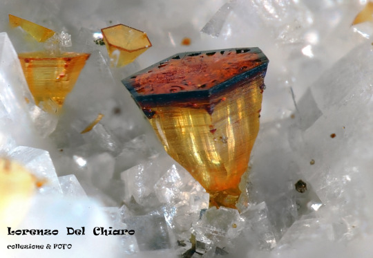
Wurtzite, Carrara Alpi apuane, photo by Lorenzo Del Chiaro
49 notes
·
View notes
Text
When we communicate with others over wireless networks, information is sent to data centers where it is collected, stored, processed, and distributed. As computational energy usage continues to grow, it is on pace to potentially become the leading source of energy consumption in this century. Memory and logic are physically separated in most modern computers, and therefore the interaction between these two components is very energy intensive in accessing, manipulating, and re-storing data. A team of researchers from Carnegie Mellon University and Penn State University is exploring materials that could possibly lead to the integration of the memory directly on top of the transistor. By changing the architecture of the microcircuit, processors could be much more efficient and consume less energy. In addition to creating proximity between these components, the nonvolatile materials studied have the potential to eliminate the need for computer memory systems to be refreshed regularly.
Their recent work published in Science explores materials that are ferroelectric, or have a spontaneous electric polarization that can be reversed by the application of an external electric field. Recently discovered wurtzite ferroelectrics, which are mainly composed of materials that are already incorporated in semiconductor technology for integrated circuits, allow for the integration of new power-efficient devices for applications such as non-volatile memory, electro-optics, and energy harvesting. One of the biggest challenges of wurtzite ferroelectrics is that the gap between the electric fields required for operation and the breakdown field is very small.
Read more.
#Materials Science#Science#Data storage#Electronics#Computing#Ferroelectric#Wurtzite#Carnegie Mellon#Penn State
10 notes
·
View notes
Text
Wurtzite Structure
Introduction
The Wurtzite structure, named after the mineral Wurtzite, is a crystal structure common to many binary compounds. It represents a hexagonal close-packed array (hcp) and is a variant of the zinc blende structure. The structure is common to many semiconductors such as GaN, ZnS, and ZnO.
Basic Description of Wurtzite
The Wurtzite structure can be viewed as two interpenetrating…
View On WordPress
0 notes
Text
Guayaco pasivo
Sex parties chicago
Cute Brunette Girl Sucking Dildo on Webcam
Cute vixens fucking in POV porn scenes
Misty Mundae kidnapped and strangled
Gays on web camera provide blowjob and nudity in sexy scenes
Tgirl whore gets analized
loiras safadas transando demais
Cumtribute for this shemale
Horny Lesbian Beauties Abella Danger And Sammie Six Cream Their Wet Cunts!
#opposable#nosebands#andamento#forestallment#long-axed#Nesconset#signitor#wurtzite#probonus#megalopine#necronite#Kurilian#Schwenkfelder#refluous#self-convened#giantism#baiza#cold-weld#north-east#nonhostile
0 notes

Text
Ways a rebellion could work
-Somehow sway Alpha Blue to actually fight back but that’s nearly impossible
-Diamond sized fusion deals with them but only two gems are meant to fuse normally so yeah
-Gems on colonies get convinced to fight back altogether and cut off the diamonds connection to said colonies
-Important gems with a direct connection to the diamonds get held hostage
-The diamonds are unable to produce new gems because the kindergartens keep being targeted
-The main thing each diamond does gets disrupted like stellar stations being taken over or the lunar station being taken over etc
-Convince Blue and Red to fight and watch them kill each other then one remains jk
-Weapons made out of Wurtzite or you actually find a Wurtzite somehow to personally shatter those lazy rocks
here you go @surelynotaconspirator
4 notes
·
View notes
Text
The present study aimed to investigate the structural, morphological, elemental, optical properties and photocatalytic activity of the bare zinc oxide (ZnO) and Manganese-doped zinc oxide (Mn- ZnO) nanoparticles (NPs) using terasil blue (TB) dye as a model substrate.
Materials and Methods: The ZnO and Mn-doped ZnO catalysts were synthesized using the co-precipitation method. The synthesized photocatalysts were characterized by X-ray diffraction (XRD), energy dispersive X-ray (EDX), and scanning electron microscopy (SEM). The band energies were measured using ultraviolet-visible (UV-Vis) spectrophotometry.
Results: The results obtained from XRD, EDX, SEM, and UV-Vis analyses demonstrated a successful synthesis of bare and Mn-doped ZnO nanoparticles. The diffraction patterns for the synthesized ZnO and Mn-doped ZnO photocatalyts were matched with that of the standard hexagonal wurtzite structure of the standard ZnO catalyst. The average particle size for the ZnO and Mn-doped ZnO catalysts were found to be 23.46 nm and 24.38 nm, and band gap energies of 3.28eV and 3.09eV, respectively. The photocatalytic performance of the Mn-doped ZnO photocatalyst was optimized using box behnken design of response surface methodology under visible light irradiation. The operational parameters involved TB initial concentration, catalyst dosage, initial pH, and irradiation time. The optimum photodegradation efficiency of TB dye removal was achieved at 96.75% of 15mg/L of TB concentration, 0.1g/L of Mn-doped ZnO, pH = 10, and 160 minutes of irradiation time. Moreover, the photocatalytic degradation of TB over the Mn-doped ZnO nanoparticles followed the pseudo-first-order kinetics model (k = 0.0254 min-1).
Conclusion: Finally, the evaluation of various scavengers confirmed that the photogenerated holes and hydroxyl radicals were the major radicals for the TB photodegradation over the Mn-doped ZnO nanoparticle under visible light irradiation.
instagram
0 notes
Text
0 notes
Text
0 notes
Text
əbdtgəæpdrətrbəellun
Pronounced: uhbdtguhapdruhtrbuhellun.
Pantheon of: substantiality, human nature, duality, individuality, impracticability, compulsiveness, seriousness.
Entities
Mnɑərʃiaɪðəmɛsnæɛʒənz
Pronounced: mnahuhrshiaithuhmaysnaayzuhnz
Seriousness: sedateness.
Impracticability: infeasibility.
Compulsiveness: workaholism.
Individuality: peculiarity.
Prophecies: electrification, runup, restriction.
Relations: nnəəwtɑsbtɒhəɪærsmʌr (corundom).
Nnəəwtɑsbtɒhəɪærsmʌr
Pronounced: nnuhuhwtahsbtouhuhiarsmur
Seriousness: committedness.
Impracticability: infeasibility.
Compulsiveness: workaholism.
Individuality: peculiarity.
Legends: reform, case study.
Prophecies: open primary.
Relations: rktvɪtikrtrðɑəkbŋægi (frequency), mnɑərʃiaɪðəmɛsnæɛʒənz (siderite), əsʃəsɑltnislvirɛkkɪr (coca cola), əʃklvraɪəɑrpərəstɛzin (eponym).
Rktvɪtikrtrðɑəkbŋægi
Pronounced: rktvitikrtrthahuhkbngagi
Seriousness: graveness.
Impracticability: infeasibility.
Compulsiveness: obsessiveness.
Individuality: singularity.
Legends: carol.
Tktrnkɪɪnkɪmrwvʃiəoæ
Pronounced: tktrnkiinkimrwvshiuhoa
Seriousness: sedateness.
Impracticability: infeasibility.
Compulsiveness: obsessiveness.
Individuality: peculiarity.
Legends: imitative electronic deception, wake.
Prophecies: carrot.
Relations: mnɑərʃiaɪðəmɛsnæɛʒənz (benefit), əsʃəsɑltnislvirɛkkɪr (zanzibar copal), əʃklvraɪəɑrpərəstɛzin (endorphin).
Əsʃəsɑltnislvirɛkkɪr
Pronounced: uhsshuhsahltnislviraykkir
Seriousness: committedness.
Impracticability: infeasibility.
Compulsiveness: workaholism.
Individuality: singularity.
Prophecies: oil change, hostilities.
Relations: mnɑərʃiaɪðəmɛsnæɛʒənz (raw umber), rktvɪtikrtrðɑəkbŋægi (calcium carbide), nnəəwtɑsbtɒhəɪærsmʌr (histidine), əʃklvraɪəɑrpərəstɛzin (wurtzite).
Əʃklvraɪəɑrpərəstɛzin
Pronounced: uhshklvraiuhahrpuhruhstayzin
Seriousness: graveness.
Impracticability: infeasibility.
Compulsiveness: obsessiveness.
Individuality: peculiarity.
Legends: mudra.
Prophecies: combination, deal.
Relations: tktrnkɪɪnkɪmrwvʃiəoæ (hidden reserve), əsʃəsɑltnislvirɛkkɪr (hemiacetal), rktvɪtikrtrðɑəkbŋægi (acetic acid).
0 notes
Text
The Morphological Properties of Zns Nanoparticles Deposited on Glass Substrates as a Function of Aluminum Content
Authored by: A A Ahmed
Abstract
The pulsed-laser deposition (PLD) method was used to deposit undoped zinc sulphide (ZnS) and Al-doped zinc sulphide (AZS) films on glass substrates (GSs). The aluminum content in the ZnS films varied from 0% to 8%. The film morphology was studied using atomic force microscopy (AFM). The films were optically characterized using an Ultraviolet–Visible-near-infrared (UV-VIS-NIR) spectrophotometer with photon wavelengths ranging from 300 to 600nm. The average roughness (Sa), root-mean square (RMS) roughness (Sq), surface skewness (Ssk), and surface kurtosis (Suk) parameters of the samples were determined using the AFM method. The samples’ AFM grain sizes were found to be 4.89 nm, 5.65 nm, and 12 nm, respectively. The doped ZnS thin film’s surface roughness was found to be greater than the undoped ZnS thin film’s. The samples showed a high transmittance across the whole visible spectrum, according to the UV data. The film optical refractive-index (n) and the extinction-coefficient (k) was computed using UV–VIS spectroscopy data. The techniques used in these investigations have been described and explained in detail. Good agreement was found when comparing results from this work against previously published data.
Keywords: Thin film; PLD; AFM; UV; Surface roughness
Abbreviations: The Pulsed-Laser Deposition; AZS: Al-Doped Zinc Sulphide, GSs: Glass Substrates; AFM: Atomic Force Microscopy; UV-VIS-NIR: Ultraviolet–Visible-Near-Infrared; RMS: Root-Mean Square; Ssk: Surface Skewness; Suk: Surface Kurtosis
Introduction
The metal chalcogenide in their crystalline state possesses many outstanding properties and has attracted considerable attention in the literature [1]. Semiconductor nanoparticles (SCNPs) films made of II-VI compounds have distinct properties that make them suited to several devices and applications [2]. Tin dioxide (SnO2), titanium-dioxide (TiO2), cadmium-sulphide (CdS), cadmium-tellurium (CdTe), cadmium-selenide (CdSe), zinc selenide (ZnSe), zinc-oxide (ZnO), and zinc tellurium (ZnTe) are all well-known SCNPs and well-studied in detail [3-10]. Among the SCNPs, ZnS is one in particular that has been widely used for a variety of applications. ZnS is an easily accessible, nontoxic, and environmentally safe compound with a higher direct band-gap energy (3.7 eV) [11].
ZnS is a metal chalcogenide with a high refractive index, a large band-gap energy, and a high UV-visible transmittance [12,13]. The polytypes of ZnS are cubic-zinc blende (sphalerite) and wurtzite (hexagonal) [11]. Furthermore, ZnS structures frequently crystallize in space groups (F43m) and (P63) in the cubic zincblende (ZB) phase at low temperatures, and (P63) in the hexagonal zincblende (ZB) phase at high temperatures [11]. Several research groups have attempted to dope ZnS films with elements such as In, Al, Fe, Co, Pb, Cd, Cu, Mn, Cr, Ni, Eu, Sm, and Cl throughout the growth process [14-20]. However, there have been infrequent studies on aluminum doped with ZnS films and placed on substrates [21,22]. However, aluminum doped ZnS films deposited on glass needs further investigation. Numerous deposition techniques, including sputtering, thermal evaporation, spray pyrolysis, chemical bath deposition, close-spaced evaporation, electron beam evaporation and pulsed laser deposition have been used to prepare ZnS thin films [14,23-26].
To our knowledge, only a few investigations was conducted on zinc sulphide thin films prepared via the PLD method on glass substrates. Several methods are demonstrated, but the pulsed laser deposition technique is shown to maintain the desired composition in the deposited thin films. Because the high kinetic energy of atoms and ionized particles in the laser-produced plasma, the PLD method can be used to deposit ZnS film at low temperatures [27]. This method is used to deposit materials on large surfaces under air conditions and on a variety of substrates in a well-controlled manner. Nonetheless, due to the intricate growth mechanism and method, deposition of ultrathin ZnS and AZS films via PLD remains extremely challenging. The results of these analyses, performed by utilizing the AFM method and the UV–Vis spectroscopy, have been documented.
Materials and Methods
Sample preparation
Sigma-Aldrich analytical grade reagents, chemical, and sodalime glass substrates were purchased and used without further purification in this investigation. The precursors for Al, S, and Zn were aluminum chloride hexahydrate (AlCl3.6H2O), thioacetamide (CH3CSNH2), zinc acetate dehydrate [Zn(CH3COO)2, 2H2O)], and ethylenediamine (NH2CH2CH2NH2) of analytical reagent quality. For several minutes, the zinc-acetate and ethylenediamine were mixed and agitated to obtain a clear and uniform solution. The product was then added to the zinc-acetate solution, followed by the addition of tri-sodium citrate. The resulting solution was agitated for a few minutes in each case. Following this, it was added to the previously produced thiourea solution while stirring. To obtain Al-doped ZnS (AZS) samples, the combined materials were mixed in the proper ratio and then dried. Numerous hours were spent extensively rushing the combined AZS samples. To manufacture the pellets of the thin films, a 5-ton hydraulic press was used for 3-5 minutes at room temperature.
Thus, pellets roughly 1.2cm in diameter and 0.2cm thick were produced from the given AZS sample. The glass substrates were degreased for 12 hours prior to deposition using soap water and alcohol. Following this procedure, glass substrates (GSs) were ultrasonically cleaned for 10 minutes with alcohol and deionized water. Finally, the glass slide substrate was rinsed, washed with deionized water, and air dried. PLD with a focused Q-switchedneodymium- doped yttrium aluminum garnet (Nd: Y3Al5O12) was used to deposit the ZnS and AZS films on the glass substrates (GSs) (Nd: YAG). The depositions took place at four-hour intervals.
Pulsed-laser ablation was carried out using a focused beam in TEM00 mode laser with primary and secondary harmonic outputs at 1064 and 532nm, respectively. The laser system was operated using pulses with a duration of ten nanoseconds. A pulsed laser with an energy density of 2 J/cm2 and a frequency of 6 Hz was used to irradiate the object. The thin film target spun as the laser restored across an area of approximately 0.5cm2 with a spot size of 3 mm2 and an incidence angle of 45°.
Throughout the development process, the target-substrate distance was maintained at a constant of 2.0cm. The substrate was clamped to a heated holder, and the temperature of the deposition solution was measured. Prior to heating the source, the chamber was evacuated to a pressure of 10-3 torr. The ZnS and AZS film were deposited on the GSs using 500 pulses and 100 mJ/pulse energy. The target and laser source were separated by a predetermined distance of 12.0cm. All films were of a thickness of between 200 and 250nm. However, when the films were grown using the PLD method, the deposition rate was calibrated, in order to regulate the thickness. The details concerning the set-up of the PLD method experiment have been provided elsewhere [14]. All samples were labeled as a control (ZnS/GSs or S0), the Al-doped ZnS/GSs (ZnS/ GSs: Al 4% or S1) and the (ZnS/GSs: Al 4% or S2), respectively. The sample morphology and optical properties were measured by the AFM [28] and the UV–Vis spectrophotometer [29].
Results and Discussion
The surface roughness of the films, as defined by arithmeticmean height (Sa), root-mean square height (Sq), skew (Ssk), and kurtosis (Sku), was measured and is shown in table 1. The film arithmetic mean height was calculated to be S0 (5.509nm), S1 (9.964nm), and S2 (23.92nm), in that order. It was observed that in comparison to S0, the Sa of the sample surface increased from 5.509nm to 23.92nm with aluminum doping. The film root-mean square roughness was calculated to be S0 (7.251nm), S1 (13.30 nm), and S2 (44.11nm), in that order.
The sample skewness was found to be S0 (0.7310), S1 (1.179), and S2 (3.585), respectively. The sample kurtosis was S0 (5.046), S1 (10.38), and S2 (20.36), respectively. These findings show that the doped sample surface of S1 and S2 was rougher than the S0 surface. The dopant of ZnS/glass substrates led to a slight alteration of the parameters. However, the Sa and Sq film parameters had increased. Furthermore, the Ssk and Sku parameters of the film increased from 0.7310 to 3.585, and from 5.046 to 20.36, respectively.
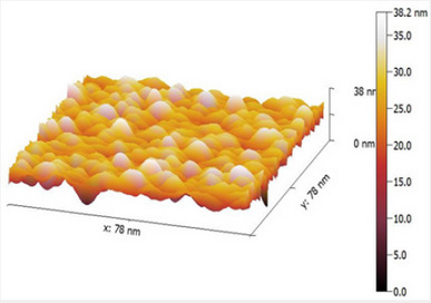
AFM micrographs of the prepared films show that spherical shape grains are uniformly distributed. Surface kurtosis values greater than 3 were found in all the examined samples, indicating sharper peaks and longer, fatter tails in general. Rku values greater than 3 indicate that the peaks and valleys have further flattened out. This finding suggests that Rsk can be used to distinguish the roughness profiles of the two surface processes. Surface roughness analysis was performed by capturing 3-D images of the surfaces of ZnS thin films with a scan area of 7.8nm x 7.8nm.
Figure 1 depicts the 7.8nm x 7.8nm 3-D images of the undoped and doped ZnS thin film surfaces for (a), (b), and (c), respectively. It is observed that Al doping induced noticeable changes in the surface morphology. The size of the grains increased for 4 wt. % Al doping (Figure 1(b)), and bigger clusters were formed on the film surface for 8 wt. % a Al doping, as shown in figure 1(c). It was also reported that Al doping in ZnS led to an increase in the grain growth.
The scales of the Z-axis in figures 1a-1c show that the surface of the undoped deposited ZnS thin film is much flatter, in comparison with the surface of the doped deposited ZnS thin film (c). When the aluminum content is gradually increased, the scales of the Z-axis of the undoped deposited ZnS thin film surface increases. It is seen in figures 1a-1c that the scales of the Z-axis are different. Figure 2 depicts a histogram of the percentages of ZnS and ZnS: Al as a function of grain size (a to c). The AFM analysis extracts surface parameters from the AZS thin films, allowing for the investigation of the surface analysis with numerical data.
The profiles of the AFM image cross section are shown in figure 2. The AFM image cross-section shows that islands in samples grown with aluminum concentrations of 0%, 4%, and 8% have a quasi-rounded shape distribution with an RMS value of 4.89nm and 5.65nm, for 0% and 4%, respectively. In contrast, for an aluminum concentration of 8%, the profiles exhibit a quasitriangular distribution of islands with an RMS value of 12nm.
The origin of the rough surface morphologies is correlated to the enhanced aluminum at a high aluminum concentration of 8%. Small ZnS islands tend to coalesce into larger ones as a result of the extra aluminum migrating on the surface. This coalescence allows for a reduction in the density of ZnS islands. Thus, 0% aluminum concentrations favor the 2D-like growth of ZnS, resulting in a wavy surface.
A quantitative optical model was employed in the calculation of the concentration-dependent reflectance of AZS structures, as detailed below. The experimental results add to our understanding of the relationship between aluminum concentrations and optical properties. A UV–Vis–NIR spectrophotometer in the 600 nm range was used to measure the optical properties of AZS thin films at room temperature. The reflectance spectrum was obtained using a UV–Vis–NIR spectrophotometer. The effects of variables on roughness were investigated using both morphological and optical responses. Table 2 shows a more detailed comparison of the films’ refractive index (n), extinction coefficient (k), reflectance (R), and surface roughness (Sa). However, as the refractive index, extinction coefficient, and reflectance of a material decrease, the value of its surface roughness increases.
In summary, we provide a correlation between Aluminum concentration and surface morphology evolutions versus the optical parameters of AZS on substrate based on the optical properties results. The results show that the high-density island structure acts to increase the scattering of the AZS surface. Changing the concentration of Al can affect the density and size of islands.
We compare the surface roughness, aluminum content, and reflectance as shown in figure 3. It is significant to note that the contribution of all surface defects and features is regarded as the primary cause of light scattering, as a result of which reflectance decreases for reflectance measurements. Finally, based on the reflectance data, we present a correlation between AZS concentration and surface morphology.
Conclusion
In summary, un-doped and Al-doped ZnS film was deposited on glass substrates using the PLD technique. The effects of aluminum concentration on the morphological and optical properties of the films were investigated using AFM and UV methods. According to the AFM studies, the film roughness changed significantly, following dopant treatment. The average roughness, rootmean square roughness, line skewness, and kurtosis of the ZnS films deposited on the glass substrates slightly increased after aluminum content-treatment. The AFM topography of doped and deposited films with aluminum content ranging from 0% to 4% revealed a surface texture with waviness.
To Know More About Juniper Online Journal Material Science Please click on:
https://juniperpublishers.com/jojms/index.php
For more Open Access Journals in Juniper Publishers please click on:
https://juniperpublishers.com/index.php
#Juniper Publishers#Material Science#Materials Theory#Structural Materials#Juniper publisher reviews#Juniper publisher journals
1 note
·
View note
Text
Fully Noninvasive Esophagectomy Versus A mix of both Esophagectomy pertaining to Esophageal and also Gastroesophageal Junctional Most cancers: Specialized medical and Short-Term Oncological Benefits
02) and also serialized cross-sectional treatment reports (suggest Realmente es: -0.Thirty three; 95% CI: -0.Fifty seven, -0.09; S Is equal to Zero.09), nevertheless non-significant reduction in RCTs (imply Realmente es: -0.Fifteen; 95% CI: -0.Thirty five, Zero.'07; S Equals 2.16) as well as pre- along with post-intervention reports (mean Realmente es: -0.30; 95% CI: -0.Sixty nine, Zero.12; S = 2.20). Heterogeneity has been big throughout these types of 15 reports (I-2 Is equal to Seventy seven.5%; P less space-consuming than 0.01), mainly due to pre-and-post input scientific studies as well as successive cross-sectional treatment reports. A conclusion: Peer-led Human immunodeficiency virus elimination surgery decreased selleck the entire UAI between MSM, nevertheless the efficiency diverse by simply examine layout. More RCTs are necessary to assess the effect of peer-led surgery while reducing potential tendency.In this study, the epitaxial expansion of (14 (Two) over bar0) ( a-plane) Zn(1-x)CdxO slim motion pictures upon (10 (One particular) around bar2) ( r-plane) pearl substrates had been completed by metal organic substance deposit (MOCVD) with the exact same cadmium stream. The actual influence regarding growth temperatures (Eight hundred fifty certifications H smaller as compared to Equals T-g smaller as compared to Is equal to 950 degrees Chemical) and also situation involving trial inside the MOCVD reactor about the microstructural and eye attributes regarding Zn(1-x)CdxO skinny films had been researched making use of high res X-ray diffraction (HRXRD), scanning electron microscopy (Search engine marketing), eye indication proportions and also photoluminescence spectroscopy (PL). An optimal Cadmium development with regards to 5.5% is obtained with T-g Is equal to 850 degrees Chemical to the taste inserted being a local reactor source. X-ray diffraction research revealed that almost all motion pictures got wurtzite cycle and also a-plane (Eleven (A couple of) above bar0) movie are epitaxially produced on r-plane sapphire. The close to band-edge photoluminescence exhaust work day gradually to lessen powers while Compact disk is incorporated along with actually reaches Three.Ten eV for your maximum Compact disk content material (5.5%) at low temperature (Two Nited kingdom). Your standard striated morphology down the [0001] ZnO direction which is a normal characteristic seen in nonpolar ZnO is lost by having an boost in the actual Compact disc use articles. This morphology modify is a result of the particular very lattice deformation that is revealed by HRXRD. (H) This year Elsevier Limited and also Techna Party Utes.third.l. Most protection under the law set aside.Cialis is often a phosphodiesterase sort Your five (PDE-5) inhibitor which is found in the treating lung arterial hypertension along with impotence problems. A new hypersensitive and specific technique is described to the determination of cialis in whole blood. Cialis and its particular inner regular (protriptyline) were remote in the matrix by sound period removing, as well as were assessed by simply gas chromatography/mass spectrometry (GC/MS) soon after derivatization by simply In,O-bis(trimethylsilyl)-trifluoracetamide (BSTFA) together with 1% trimethylchlorsilane (TMCS). Limitations associated with discovery as well as quantification pertaining to tadalafil had been Zero.75 and a couple of.Double zero mu g/L, correspondingly. The calibration curve was straight line involving A couple of.50 along with Five-hundred.0 mu g/L, with a correlation coefficient more than 3.991. The price acquired regarding intra- along with inter-day accuracy was discovered being in between -10.5 to 8.
0 notes
Text
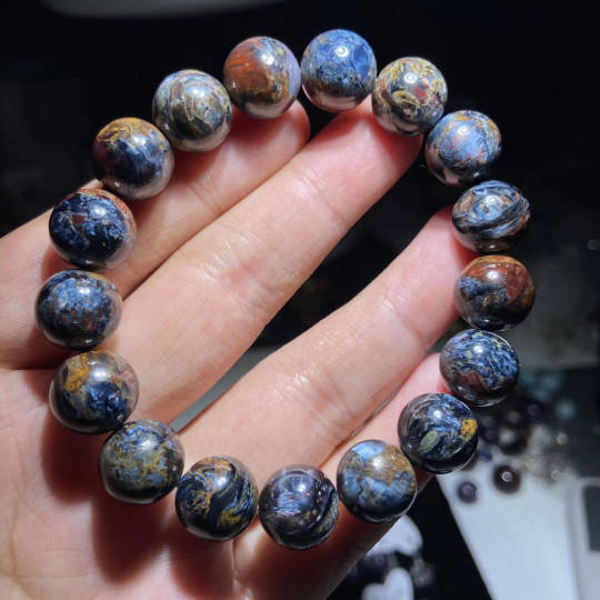
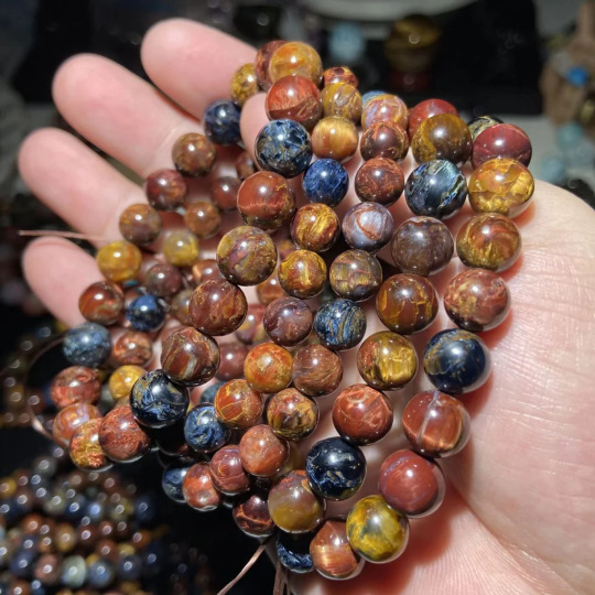
Main Components and Morphological Characteristics of Pietersite
The main components of Pietersite:
The original mineral components are mainly alkaline and alkaline earth amphibole asbestos, including magnesium sodium amphibole asbestos, calcium magnesium sodium amphibole asbestos, sodium aluminum actinolite asbestos, tremolite asbestos, sodium actinolite asbestos and actinolite asbestos.
The main mineral compositions are: chalcedony, quartz, sometimes associated red, white agate and onyx, opal, trace specularite, pyrite, hematite (limonite), albite, calcite, barite, and wurtzite. The chalcedony is a colorless cryptocrystalline aggregate with greasy luster. From the appearance, the chalcedony tends to bond or wrap blue asbestos after the formation of blue asbestos, making it a colorful tiger eye mineral. The presence of iron oxide makes Pietersite show different colors. Blue asbestos fiber, which is not weathered or iron stained, is blue; Those that have been mineralized by ferritization are purplish red; The weathered ones are golden yellow. The minerals in the blue asbestos veins show obvious zoning and other functions.
Morphological characteristics of Pietersite:
The products developed by pietersite are all inclusive. If you watch this product in detail, you will be happy to forget about the world of strange magic colors. For example, the scenic brand can be said to be the living color of the earth's activities and changes over thousands of years. There are spectacular scenes of volcanic eruptions, as well as flowing magma flashing red, yellow and gold; It also seems that there are various natural materialized art color changing patterns, which are very beautiful. Pietersite symbolizes safety. The jewelry produced has the effect of cat's eye (moving light and shadow), and also looks like the bright eyes of a tiger. Because of its majestic spirituality, it is sacred and inviolable, and is considered to be a gem for eliminating disasters and evil spirits, and for attracting good luck. Wearing gems can improve decision and creativity. It is inspiring to make progress.
Like opal, it has obvious and unique features, like stern eyes, more like mysterious boundaries. From different angles, it differs from opal in that the color of Peter's cat's eyes is more domineering and gorgeous.
Since ancient times, it has always been a gem that people yearn for and want to own.
In this ore group, a series of colorful ore bodies have been formed due to different growth environments and trace elements. The common ore is brown yellow, while the blue gray and red brown are few. Among them, the ones with clear, bright and complete eyeliner, good gloss and clear grain, no impurities on the stone, uniform texture and best color. It is considered as a treasure of nature and a miracle of the earth. The unique gem structure is like the eyes of an elf, flickering, mysterious and colorful, full of spirituality, and represents the life endowed by nature.

0 notes
Text
Disk led free

DISK LED FREE FREE
We derive the effective-mass Hamiltonian for wurtzite semiconductors, including the strain effects. This strain confinement mechanism is the origin of the luminescence quenching in very thin GaN quantum disks, as well as the main source of the emission linewidth broadening. This strain reduction annihilates partially the piezoelectric field, giving rise to a specific carrier confinement mechanism (strain confinement), that depends on the disk thickness.
DISK LED FREE FREE
An inhomogeneous biaxial (in-plane) strain distribution within the GaN quantum disks, pseudomorphically grown on strain-free AlxGa1-xN nanocolumns, results from a reduction of the accumulated elastic energy at the disk free surface (GaN-air boundary). Experimental emission energies are compared to theoretical calculations based on a one-dimensional Schrödinger-Poisson solver, including spontaneous and piezoelectric polarizations, surface potentials, and strain. This paper will show that NIL is an excellent technology to produce nanopatterned GaN substrates highly suitable to grow defect free arrays of positioncontrolled nanorods for ultrahigh brightness LED applications.Ĭarrier confinement effects in nanocolumnar AlxGa1-xN/GaN multiple quantum disks have been studied by photoluminescence, as a function of the Al content and quantum disk thickness. The nanopatterns created by NIL can be applied to control metal organic vapour phase epitaxy (MOVPE) growth of GaN nanorods. The mentioned irregularities are particularly disturbing when NIL based processes are utilized to create patterns onto the wafer surface. These types of substrates suffer from growth defects like hexagonal spikes, vpits, waferbowing, atomic steps and surface corrugations on a scale of few 10 mum or even large islands of irregularities. The wafers used for producing LED's are typically III/V semiconductor materials grown with epitaxial processes. One of the first application areas in which NIL is used is manufacturing of various types of LED's. Nano Imprint Lithography (NIL) is a promising technology that combines low costs with high throughput for fabrication of sub 100 nm scale features.
0 notes
Text
What Are The Factors That Affect The Thermal Conductivity Of AlN Ceramic Substrates?
First of all, let’s overview AlN Ceramics
AlN is a covalently bonded compound with a stable structure and hexagonal wurtzite structure without the existence of other allotypes. Its crystal structure is the AlN4 tetrahedron produced by the disproportionation of aluminum atoms and adjacent nitrogen atoms as the structural unit; the space group is P63mc, which belongs to the hexagonal crystal system.
The main features of aluminum nitride ceramics:
(1) High thermal conductivity, which is 5-10 times that of alumina ceramics;
(2) The thermal expansion coefficient (4.3×10⁻⁶/℃) matches the semiconductor silicon material (3.5-4.0×10⁻⁶/℃);
(3) Good mechanical properties;
(4) Excellent electrical properties, with extremely high insulation resistance and low dielectric loss;
(5) Multi-layer wiring can be performed to achieve high density and miniaturization of packaging; (6) Non-toxic, good Conducive to environmental protection.
Various factors affecting the thermal conductivity of AlN ceramics
At 300K, the theoretical thermal conductivity of AlN single crystal material is as high as 319W/(m K), but in the actual production process, due to the purity of the material, internal defects (dislocations, pores, impurities, lattice distortion), grain The thermal conductivity is also affected by various factors such as orientation and sintering process, which are often lower than the theoretical value.
In summary:
Selecting the appropriate sintering aids in the composite system can achieve a lower sintering temperature of AlN and effectively purify the grain boundaries, and obtain AlN with higher thermal conductivity.

What Are The Factors That Affect The Thermal Conductivity Of AlNCeramic Substrates
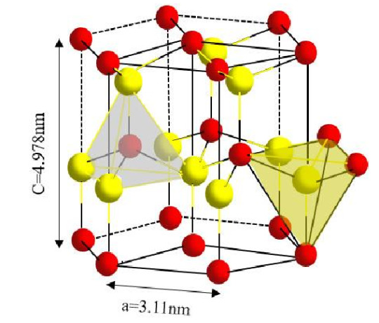
AlN Schematic diagram of the crystal structure
Read the full article
#AlNCeramics#AluminumNitride#factorsaffectingthethermalconductivityofAlNceramics#FeaturesofAlNCeramics#ThermalConductivity
0 notes
Text
10 Strongest Material in the World
Strength means an ability to withstand stress. A material is termed as strong if it can withstand a large value of stress without getting fractured. Recent developments in material science have introduced amazing materials which have a large value of tensile strength. Some are very light hence their strength-to-weight ratios are very good and can surpass Kevlar and even diamond. So here is our list of 10 strongest materials.
10. Palladium Alloy Glass
9. Ultra-High-Molecular-Weight Polyethylene (UHMWPE)
8. Limpet Teeth
7. Zylon
6. Moissanite
5. Diamond
4. Wurtzite Boron Nitride (w-BN)
3. Lonsdaleite
2. Carbon Nanotube Paper (Bucky Paper)
1. Graphene
0 notes
Last Seen Blogs

shrubsparrow
The Shrubbery

sidigame9g
Sidigamee9g

this-is-sar
Bribes

lanxuan-ts
LanXuAnbaby

revelbvnl1
Untitled