#Large PCB
Text
How do PCBs automatically help power with conductive pathways for non-conductive substrates?
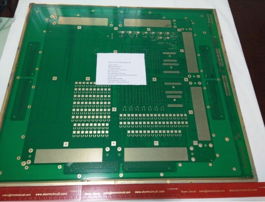
HDI 12-layer PCBs automatically powered to help are called PWB (Printed wiring boards), PCBs (Printed Circuit Boards) come accessible to automatically help and electrically be part of electric powered-powered utilization of conductive pathways, signal strains etched from copper sheets laminated onto a non-conductive substrate. Apart from being much less high priced and reliable, PCBs are used for immoderate-volume production, even though their price is higher than wire-wrapped circuits. Generally, a Printed Circuit Board’s format is ready vaguely. Important characteristic internal PCB circuit format this is carried out to define the functionality further of mechanical and electric-powered products. This microwave PCB Prototype plays a crucial element characteristic within the format and introduction of found-out circuit boards. The technique of the PCB prototype goes via immoderate situations the whole thing is checked on the equal time because the manufacturing is in a technique including the strains and leads. However, underneath any kind of failure within the prototype, a present-day modified prototype needs to be built.
How are PCB prototypes to scrutinize efficiencies?
The prototype is saved under scrutiny until it performs as required. In case of the unavailability of a prototype of the Printed Circuit Boards, there are various uncertain risks and inefficiencies worried about the mass production of circuit boards. These revisions additionally may be time-ingesting in complex systems and may include immoderate expenses. Also, if something is determined incorrectly with a circuit, it takes a while to localize it. Different ENEPIG PCB materials are used for sort of PCB specifications and techniques in PCB prototyping and production.
What are the power outputs of rigid-flex PCB?
To get wonderful consequences and outputs, you will be capable of creating or formatting a PCB with the utilization of
Using Polyimide for flexibility – Polyimide can keep a heat temperature, which makes it most suitable for use in electric insulation applications.
Arlon for Longer Life at Higher Temperatures – Arlon materials are useful for the PCB fabrication of immoderate ordinary overall performance and frequency-mounted found-out circuit production.
Isola Range for PCB prototype – Isola range is an immoderate ordinary overall performance pre-peg system.
UTILITIES AND FUNCTIONS
Its low dielectric consistency and dissipation element permit the growth of an appropriate cloth for designing broadband circuits.
Last phrase and conclusion Storm pcb.com are expert in digital layout and PCB assembly. They remodel your circuit concept into reality, seamlessly, economically, and successfully for exceptional circuit manufacturing for men or woman demand.
#HDI PCB#RF PCB#High frequencypcb#rigid-flexpcb#Large PCB#Metalcore PCB#ENEPIG PCB#Microwave PCB#10 layer PCB#12 layer PCB
7 notes
·
View notes
Photo


Pretty 1889 Victorian in Salem, Virginia 4bd. 4ba. and is listed for $575K.


Enter a center hall with an intricately carved stairway.


Lovely sitting room with a mantel and heat stove. Check out the artwork on the fireplace surrounds.

In the dining room is a beautiful chandelier and a painted fireplace surround.

The room outside the kitchen is being used as a bedroom with another fancy fireplace.

There’s a shower room on the first floor with a nice pedestal sink.

There is also another nice bath with a tub.

A back porch entrance with rear stairs to the 2nd fl.

There’s a mudroom closet back here.


The kitchen remodel has nice cabinetry and that burgundy stove.

Vintage looking wallpaper and nice white heat stove, too.


Moving on to the 2nd level and bedrooms.


Large secondary bd. I can’t get over the fireplaces in this home and I’m wondering if that’s an original closet.

There is a small full kitchen up here.

This large bd. must be the main one, b/c it has an en-suite.


Next to the main bd. is a secondary bd., also very large.


All 4 bds. are very large.

And, this is the 4th of the 4 baths. It has a bit of a vintage look.

The is nice- a 2nd fl. porch. I wonder what’s behind the small door- could be storage.

Or, it could lead to the attic. The attic is interesting- it’s not completely finished, but it’s unusual and being used.


There’s a cement patio in the back of the house, with a private fence surrounding the area.


There’s a nicely sized yard of .40 acre.

There’s no pool, but the hot tub is pretty big.

Plus a driveway with an old cement single car garage.
https://www.facebook.com/photo/?fbid=658093629696043&set=pcb.658101956361877
473 notes
·
View notes
Text
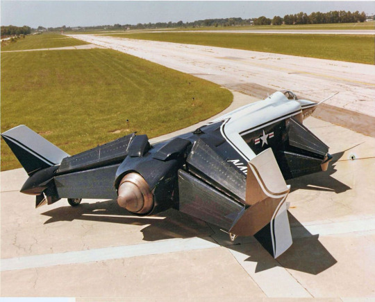
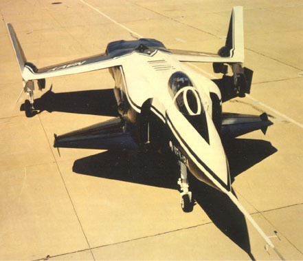
Rockwell XFV-12A

Rockwell XFV-12A
by Alex Stoll

Around 1970 the Navy could not see how it was going to be able to replace its old Essex and Midway carriers with Nimitz-class supercarriers. Admiral Elmo Zumwalt directed a study of alternatives which resulted in the Sea Control Ship (SCS), a mini-carrier equipped with V/STOL fighters and ASW aircraft. The USN invited manufactures to propose demonstration programs for a new aircraft, called the V/STOL Fighter Technology Prototype, to replace the outdated Harrier and serve on the SCS or other ships much smaller than conventional carriers: BAe and MD proposed an improved Harrier and a supersonic Harrier with a PCB (Plenum-Chamber Burning) engine; Boeing and Northrop proposed jet-powered tail-sitters; Lockheed-California proposed a propeller-driven tail-sitter; and Rockwell proposed a canard-delta aircraft powered by a large and enormously powerful engine that used the ejector-lift system for V/STOL. The Navy awarded the contract to Rockwell in 1972, instead of choosing designs based on proved technology, and the XFV-12A designation (twelth in the V series, not in the F series; the F-12 was the interceptor verison of the Blackbird) was allotted. Even though the forward fuselage and landing gear of the A-4 and the wing box, air intakes, and fuel tanks of the F-4 were used to speed the program up, it still ran far behind schedule. The prototype was rolled out in December 1976 and the first flight was scheduled for 1979.

Engine Configuration
For takeoff and landing, the entire engine was ducted to hollow-section "ejector flaps" (also called augmentor flaps) out along the wings and the canard by pilot command via a diverter valve box. The high-energy hot gas forced fresh air from above through the ejector flaps at a ratio of 7.5:1 to boost thrust by 70 percent. The ejector flaps could be raised or lowered to provide a smooth transition from vertical to horizontal flight or vice versa. After the XFV-12A's cancellation, de Havilland Canada designed an aircraft with ejectors build into the roots of a delta wing. GD incorporated their concept into the E-7, a F-16-based delta-winged STOVL aircraft. DHC built a large powered model and tested it in 1987. The EL system was large and control was difficult as a result of the large air mass moving through the wing root during transition, and nothing came of it (though not because the EL couldn't produce enough thrust as in the XFV-12A's case) despite the attractive low exhaust velocity.

Cancellation
Rockwell and Pratt & Whitney experienced several major technical problems, and the thrust boost from the ejector flap system was never as large in the full-scale aircraft as predicted from data collected by test rigs and sub-scale models; the XFV-12A could not leave the ground. Eventually funding dried up, the SCS was canceled, and the program proved a disappointment; however, in most future ASTOVL programs, large-scale powered models were used because of the experience gained in the XFV-12A program.
123 notes
·
View notes
Text
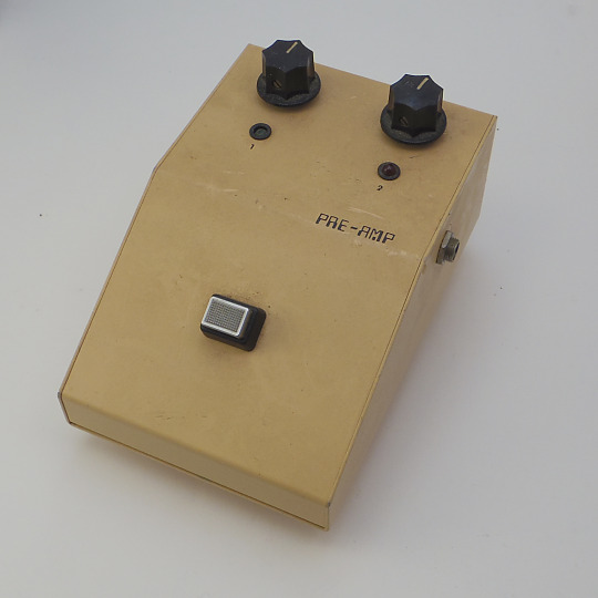

AMZFX - PRE-AMP
"This is a dual op amp booster that was the predecessor to the dual op amp pcb that I sell on my site. I'm not sure how old it is but it pre-dates the internet! I used this pedal sometimes when playing live.
A tap of the footswitch toggles between the two channels that can be set for different gains.
The enclosure is a folded sheet-metal aluminum box that was widely available. It is a little large compared to modern pedal builds. The power supply jack is a 3.5mm phone jack style socket, such as was used on the original Rat pedals. The bypass is a soft-touch electronic switch circuit using a cmos chip. This was before microprocessors became very small and cheap, but cd4066 cmos switches cost pennies and were available everywhere."
cred: muzique.com/dual-boost, instagram.com/amzfx
15 notes
·
View notes
Text
I got an ask about Donnie's condition at the start of the first fic and I thought this snippet of my very first notes might be interesting to someone? Usual warning for medical body horror and light mutilation but it isn't particularly graphic. Still putting it under a readmore so read at your own risk.
Pollution and over salted water have caused damage to skin inside throat used to absorb oxygen directly.
Ate a lot of European green crab, ate oyster toadfish left dead at river edge for stealing bait, own snare traps have caught dogs, rats and raccoons. Ate American eels.
Mesothermic - immune to rabies
Carries but is not affected by salmonella bacteria
Cadmium poisoning - lung damage (rales, coughing sometimes to the point of blood specks)
Lead poisoning specifically causes tremors in hands and limits mobility. Contributed to developmental delays exacerbated by almost full isolation.
PCB - liver damage (enlarged liver, high enzymes), chloracne (cysts/keratin plugs across shell, thick & peeling skin around eyes. Initial pain reaction high when thickened scale peeled)
PFAS - another liver fucker upper, vaccine reactions, cholesterol (immune response to initial medication altered, reaction after each dosage briefly results in flu like symptoms and exhaustion, decreases as medication continues)
Blood Flukes - mostly reduced to eggs within bloodstream, additional traces of liver damage
Nematodes- severe outbreaks result in coughing and vomiting worms, underweight, dehydration. Worms mutated by trace amounts of Empyrean in system. Infestation started within the first month of solitude, population evolved. Regular nematodes introduced would now be devoured. (Almost symbiotic, mutated nematodes prevent further infestations of other parasites in the digestive system.)
Eosinophilia (high white blood cell count)
enterococci (fresh/salt water e coli variant) - i don't want to go into this one actually but it definitely contributed to the low body weight.
See manatee scars: struck by boat propeller across back. Meat scooped. Skin grew back over into indentations. The healing altered the shape of the shell, turns up at edges/too small.
See softshells kept in small enclosures long term.
Face scarring- tried to climb into a rat nest and was chased out. Unaware of how to treat injuries resulted in first major infection from scratch across jaw/mouth. Scars grew with Donnie's face.
Burned hand - early experiment with electricity/generator. Lead poisoning shakes resulted in severe burn, healing caused muscle degradation.
Unable to walk on two legs. Extremely shortened calf muscles, can straightened legs but straightened legs cannot hold weight. No problems swimming or moving on all fours. Pelvis mutated towards bipedal shape but adapted.
Underweight! Refeeding syndrome risk.
Hates touch/never been comforted. both seeks out and recoils from affection.
Human mauled: looking for crocodile man cryptid and saw Donnie. When cornered Donnie lashed out. Removal of most of calf muscle, most of skin from lower leg, dislocated kneecap. Multiple ruptures to femoral artery.
Donnie doesn't know what happened to this person but does know if he survived a large portion of his leg would have been amputed. Aware that likelihood of survival extremely low. Tends to downplay this incident.
15 notes
·
View notes
Note
Still thinking about Youkai Sakuya. Letting it percolate in the brain. And the Thematics. I'm thinking like. Something has to happen that changes her personal status quo. The timeless servant serving the timeless master and occasionally solving incidents with her friends and friendly acquaintances. As much as youkai are by nature.. unchanging. Embodiments of concepts more than they are freely moving and operating beings(though they are without doubt a mix of both) there would have to be a catalyst. Something that forces her away from her connection to humanity(and towards her connection to the other and the divine) in a sudden, sharp jolt. Anything less would be course corrected. She's a tough girl.
Maybe.. something with Yukari. After a troublesome incident. Maybe with a youkai of fear, or one with the power to twist reflections. Something that would force introspection. Yukari drops a few choice words here and there(Why? I don't know. But she'd have a reason.) and pushes her over the edge while she's in a vulnerable place. Who knows what happens from there.
Just some brainworms, ultimately. I like it when women with something wrong with them are made worse(by other women).
Honestly, I think if Yukari was interested in having Sakuya being a youkai, she would've made a move about it after the vampire incident, or in PCB. She's known her for a long time, and she's been youkai-like all the while.
Furthermore, I don't think youkai are really unchanging. They don't change in the same way humans do; they don't age, or grow, or anything like that. But they adapt to new circumstances probably better than humans do; they're simply large ships on a rough sea, compared to tiny boats.
Also, a youkai of fear? The thing all youkai are youkai of?
11 notes
·
View notes
Text
((OOC rant about work under read more. Just needing to vent.
Today was like... One of those days where there were so many dumb questions. I'm usually very patient with these because my job is in the warranty department for an appliance company and I KNOW that not a lot of people would necessarily have the same technical knowledge I've acquired over time. This isn't about any of those. It's things like:
- This one lady called asking if any of our units were sold in Canada. Apparently the sales department sent her to us. I don't know WHY because I'm in the warranty department! The only things I sell are parts! I told her that we don't directly sell to Canada (we are US-based) but that I wasn't sure about any other distributors like Amazon, Lowe's, Home Depot, etc. She got mad at me like I was stupid for not knowing a SALES question and said I should know better and expected a yes or no answer. So after talking to my supervisor, who ALSO didn't know, I erred on the side of caution and said no. But she got mad at me again saying that it was a pretty large market to lose our on. LADY. I TOLD YOU I AM IN THE WARRANTY DEPARTMENT. And it's not like I have any control of where we sell our stuff. And you SPECIFICALLY wanted a yes or no answer so I GAVE you one. And it's not like we have anything against Canada, it would be more of a case where we don't sell to anywhere outside the US at all! We don't even ship to Hawaii or Alaska! Ugh.
- I got an email for a guy saying that I sent him information for the "PCB" but he needed the power board instead. Thing is, PCB stands for power control board. I would be more understanding of this if I didn't literally say the whole thing in the subject line of my original email.
- And this is on top of the usual troubleshooting stuff like "okay is it plugged in?" Stuff.
5 notes
·
View notes
Text
Mugshots of women political prisoners from Brazil


Maria Amélia de Almeida Teles, Amelinha Teles. She was arrested in 1964, and then again in 1972 with her husband, César Augusto Teles. The couple's children were also taken by the DOI, and remained there for days, witnessing the condition of their parents. + ( 9/24)

Maria Aparecida dos Santos, Cidinha. She broke with the Brazilian Communist Party – PCB (the Party), to join the ALN, a dissent from Marighella. Her capture occurred when she was preparing to leave on a trip to Cuba to undergo guerrilla training, + (7/24) then 22 years old. Her imprisonment in the Tiradentes Prison Tower lasted more than three years. + (8 /24)

When she was arrested in 1969, she was a member of the VPR (Vanguarda Popular Revolucionária). She suffered the most atrocious abuse, but resisted and managed to leave Brazil and passed through several countries, until she was the first exile to return, in 1979, with the Amnesty Law. + (6/24)

Rose was tortured and imprisoned for 9 months, and was tried and acquitted in 1972. Today she presides over the Tortura Nunca Mais Group in SP. + ( 11/24)
Women participated in the resistance to the dictatorship on the most diverse fronts: in the countryside and in large urban centers, participating in logistical actions, support activities and armed struggle. Even so, they are seen as supporting forces in the resistance to the dictatorship with men considered its protagonists.
#Tortura Nunca Mais#political prisoners#partido comunista brasileiro#brazil#military junta#Vanguarda Popular Revolucionária
3 notes
·
View notes
Text

I have this delusion that if I can make real life Doc Ock arms she'll become real and love me. So I'm gonna try and do that before I get bored and it becomes another discarded folder of CAD on my desktop.
I'm going to use electromagnets to do it, because that's one of the only ways I could think of trying to replicate the soft robotic arms from Spiderverse. (I know that's not how actual soft robotics work, but I just have a 3d printer so I'm working with what I've got) I'm starting off with a proof of concept, basically just taking an electromagnet, putting it at one end of a shell with some metal on the other end and seeing if I can compress and extend it.

I made an electromagnet calculator to get the dimensions and power requirements needed for the force I want. I originally wanted to get 100N at 75mm gap between top and bottom but that would either require a way beefier power supply or really large coils, so I reduced my expectations. I have some DC motor drivers ordered to actually run the coils and I have a old laptop power supply combined with a buck converter to drop the voltage to the correct level.


For the physical design I went with two half circles intersecting, this was to hopefully make it bend near the middle instead of the ends. I've run some basic FEA on it, but I don't have the material properties for TPU so it mostly just helped to beef up the areas near the threads to prevent them from buckling rather than getting a good simulation of how it will fold. Once I get the magnets working I'll play around with some more exotic shapes to see what works the best. I might even try adjusting the wall thickness through the height.
I just realized that I need to actually find a way to secure the spools to the little caps because right now they're just indexed with the nubs. I thought about super gluing them but I do want to be able to retrieve them at some point for use in future versions.
To actually test them I'm going to hook them up to an Arduino Nano or something with the motor drivers. To actually test how much force they're outputting I though about using a kitchen scale and seeing that way. Another though was to just get a 2kg weight and put it on it. That way if it can lift that up it fulfills the requirements I set up (20N at 75mm gap between magnet and metal). I've also though about making some sort of jig with a load cell. It would let me get more precise data but means I spend time designing and manufacturing more testing infrastructure rather than the actual project.

If I am going to be making more coils, then I might need to think about making a jig or machine for winding them. My calcs say I need coils with a couple hundred turns at least, so making a simple machine to turn them for me would save a lot of time if I want to make a lot of nodules. The main issues I see are getting
If the tests works then I'll move onto a version with four sets of magnets so I can bend the nodule (I'm calling them nodules) in any direction. I'd also like to get some PCBs for controlling them, that way I can connect them up to each other a main hub through I2C or something and collect data like temp. I also have to think about power dissipation because they could sink a good number of Watts, so if I do something funky, like have cut outs for airflow in the PCBs, then have fan at the end of the limb to push air through it could solve that. This is all way in the future though. I need to wait for all the stuff to come in and actually test it.
#doc ock#spiderverse#olivia octavius#otto octavius#engineering#project#3dprinting#mechanical engineering#doctor octopus
19 notes
·
View notes
Text
Extra Thinky Bits

Ever since I built my 68000 computer, I've used a BASIC Mandelbrot rendering program I got from RosettaCode as a test benchmark. On the 6MHz 68000 it took nearly 10 minutes to run. With the 68030 running at 56MHz using a 32-bit data bus with L1 cache enabled, the same BASIC program completed in around 14 seconds.
But we can do better. EhBASIC is written in assembly to use 32-bit single-precision floating point numbers internally, but all of its mathematical routines use the CPU's integer ALU. There are large sections of code that could theoretically be replaced by single instructions for the 68882 floating point math coprocessor (FPU).
Adding the FPU is where I stopped on my original wire-wrapped prototype. I simply never could get it working reliably. I've since learned that I had some logic errors that were probably causing more trouble than my chosen method of prototyping. But this meant it was probably best to start over, and if I'm starting over, a custom PCB with a CPLD to handle logic & timing would be much easier, much more flexible, and much more reliable.
Another tumblr user, Avics1967, had pointed out that logic error to me a while back. It turns out the 68882 FPU is picky about the setup time relationship between the FPU's Chip Select signal and the CPU's Address Strobe signal. Basically, the Chip Select signal can't be transitioning at the same time that the Address Strobe signal is falling, and there's a few nanoseconds on either side of that AS# transition where the CS# signal must be stable. My original design didn't take this into account.
This setup time target ended up being harder to hit than I anticipated. With my little system running at 40MHz, there is just 12.5ns between the CPU asserting the address bus and the CPU asserting its Address Strobe. I need to allow about 3ns for the FPU Chip Select signal to be stable before AS# falls.
I'm using a 10ns CPLD for logic.
My first draft for the logic also did not meet timing requirements, and with my bus speed and parts on hand it never would. Luckily, the 68882 also supports what Motorola called "Late Chip Select", where the CS# signal could be asserted after AS#. So that's what I ended up doing — I implement a delay synchronous to the CPU clock to assert CS# half a clock after AS#.
I ran into an interesting problem while testing though. I assembled a short program to add 2+3 and store the result in memory where I could check if the result of 5 was stored properly. What I got instead was an endless chain of bus errors. If I hit reset quickly enough I could see the very first error was actually an Address Error, and then came the endless chain of Bus Errors.
This made no sense. The FPU can generate some exceptions, like the Coprocessor Protocol Violation I had gotten with my last prototype. And if there was a problem with my logic, a Bus Error might be thrown if the FPU wasn't detected or didn't respond in time. But an Address Error?
Turns out the FPU wasn't the problem at all. There was a typo — a single missing # — in my monitor which caused the CPU to try to load an odd instruction as a pointer instead of the actual pointer to the exception handler routine. So something was indeed causing an exception, but I couldn't see what the exception actually was because it was immediately followed by an Address Error which also spawned a Bus Error.
Thankfully, my exception table is in RAM, so I was able to patch it live before running my test program. And the next time I tried testing the FPU? It worked!
I have no idea what was causing the initial exception, but the FPU has been working for me since.
Now it's time to write some more sophisticated programs to really test the FPU, and maybe modify BASIC to use the FPU instead of its built-in arithmetic functions.
37 notes
·
View notes
Text
THE METAL CORE PCB FROM STROMPCB.COM HELPS PRODUCE BEST-LED PACKAGES
Metal Core PCB are circuit forums or MCPCB, or thermal control forums are revealed circuit forums constructed with a PCB metallic middle used to disperse warmness from the additives of the board, successfully decreasing the middle temperature of excessive warmness packages. They are used while traditional fan-cooling strategies are inadequate for cooling the whole system. Most normally observed in LED packages, MCPCBs will have a middle of one of the following materials: — aluminum (aluminum middle PCB) — copper (copper middle PCB) — a combination of unique alloys With the maximum not unusual place of the 3 indexed above being aluminum middle forums. Metal middle revealed circuit forums switch warmness many times (up to eight or nine times) quicker than FR4 forums.
Retaining warmness producing cooler additives from metal core PCBs
MCPCB laminates scatter and do away with warmness, retaining warmness and producing additives cooler that ends up in multiplied overall performance and lifestyles of the packages. Common LED packages in which metallic middle forums are observed: — Back mild unit packages — Street protection packages (streetlights, lights, etc.) — General lights packages — System car LED packages — Power converters: telecom, industrial, excessive voltage regulator, electricity supplies — Hybrid/electric powered motor manage packages — Photovoltaic
Applications The mild-emitting diode packages generate massive quantities of warmness.
With the large PCB metallic middle’s dielectric polymer layer with excessive thermal conductivity, the utility average has a decreased thermal resistance. Other packages which might be turning into an increasing number of vital metallic middle forums are solar panels and movement manage packages. As sun electricity harnessing will become an increasing number vital in regular packages together with electric powered automobiles and sun panel roofs, the warmth trapped inside them increases. Likewise, with superior movement management packages, massive quantities of processing and friction are created to create the dynamics of the motion of the superior generation robots.
PCB used in electronic items
In not unusual place pc packages today, LEDs and LED indicator lighting fixtures are regularly used. The mild warmth created via way of means of those LEDs has multiplied the middle temperature of packages significantly, making the want for thermal control more and more vital. Metal middle forums are most usually observed in LED packages and also in LED-heavy pc hardware situations. MCPCBs have nonetheless fabricated the use of preferred SMT (floor mount generation — the whole frame of the method and additives that create revealed circuit board meeting with leadless additives) meeting equipment. They are commonly multi-layered forums. They also can be constructed on a flex board or inflexible flex board for tight area regions or custom-sized packages, together with cellular phones.
#HDI PCB#RF PCB#High frequencypcb#rigid-flexpcb#Large PCB#Metalcore PCB#ENEPIG PCB#Microwave PCB#10 layer PCB#12 layer PCB
1 note
·
View note
Text
since I realise that there's probably a lot of people out there who never got to etch a circuit board in school, the basic principle of how a PCB or Printed Circuit Board is made is basically this:
You take a flat board, I believe usually fibreglass, that's been coated in a thin layer of conductive material, usually copper. You then mark out which bits of copper you want to keep versus the ones you don't, either physically or in software in some form depending on your method of etching, and then basically remove all the copper you don't want from the board, before finally coating the end result in what's called a solder mask to prevent solder from sticking to every single copper trace and risking short circuits - the solder mask being what makes the board actually green (or whatever other colour - there's a number of different possible ones!)
this also means that if you take a sharp hobby knife or the like and scrape away at the solder mask, you can expose or even cut the copper traces underneath, depending on whether you want to add or sever a connection somewhere.
Note that in this example (and in many other circuit boards) there's this very large and wide trace that covers most of the board where no other traces are present that I've labelled the ground plane - those are usually connected to either positive voltage or ground (in this case to ground via pins 9 and 22) and are used to provide easy access to either power or ground, plus their width means they can also pass much more current without overheating; in fact, if we were to compare this PCB to that of, say, a 100W+ something power supply...
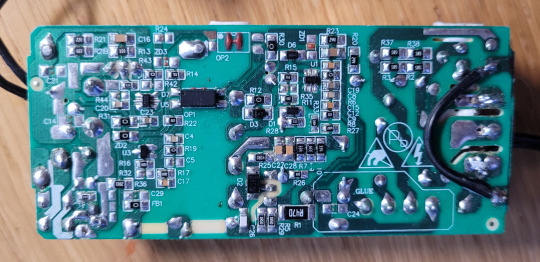
... you might notice the latter has some pretty beefy traces going around, especially towards the left and right ends of the PCB where the outputs and inputs respectively are located, due to the significant amounts of energy that might end up passing through those traces.
Meanwhile, most of the smaller traces and components are all primarily involved in regulating the behaviour of the larger and more powerful parts on the other side and therefore won't see all that much voltage or current. The big stuff is all topside and generally in contact with blocks of aluminium to act as heat sinks to prevent them from cooking themselves and releasing the magic smoke.
3 notes
·
View notes
Photo


Here’s a timeless French country home in Eagleville, Pennsylvania. Built in 1950, it has 3bds. 2ba. and is listed for $950K.


It really does make you feel like you’re living in the French countryside.


Rustic elegance.


I like this feature- the living room is above the dining area. It’s open, but separates the 2 spaces.

Love the red cabinets- just enough to make the kitchen pop.


Country French touches everywhere. The cabinets tie in beautifully, but look like random pieces that would be in a real old country French kitchen.

Coy family room.


The main bd. has an opening in the wall with a railing to overlook the first floor. Unique feature. There’s also skylight to give it lots of natural light.


Large main bath has a stone shower.

I like this- the room is neutral, but they gave it color by painting the wood trim bright pink.


The 2nd bath is so grand- look at that shower. Elegant old marble elements.

Just enough painted ivy on the wall and ceiling. So subtle.

There’s a bright bonus room in the finished attic.

Beautiful stone patio.


The home is surrounded by 4 acres of gorgeous land.
https://www.facebook.com/photo/?fbid=561511496020924&set=pcb.561512009354206
188 notes
·
View notes
Text
PCB Via Current-Carrying Capacity: Is My PCB Too Hot?

In the realm of printed circuit board (PCB) design, one of the critical factors that significantly impact the performance and reliability of a circuit is the current-carrying capacity of vias. Vias are the small plated-through holes that interconnect different layers of a PCB, facilitating the flow of electrical signals and power. However, when subjected to excessive current loads, vias can generate significant heat, leading to thermal issues and potential PCB failure.
Understanding the current-carrying capacity of vias is crucial for ensuring proper thermal management in your PCB design. In this article, we will delve into the factors that affect via current-carrying capacity, explore thermal management strategies, and provide practical tips to help you determine if your PCB is running too hot.
Understanding Via Current-Carrying Capacity
The current-carrying capacity of a via is determined by several factors, including its physical dimensions, the materials used in its construction, and the thermal environment in which it operates. When current flows through a via, it encounters resistance, resulting in the generation of heat. The amount of heat generated is directly proportional to the current flowing through the via and its resistance.
1. Via Dimensions
The physical dimensions of a via, such as its diameter and length (thickness of the PCB), play a crucial role in determining its current-carrying capacity. Generally, larger diameter vias have lower resistance and can carry higher currents without overheating. Similarly, shorter vias have lower resistance and can dissipate heat more effectively than longer vias.
2. PCB Materials
The materials used in the construction of the PCB can also affect the current-carrying capacity of vias. Different materials have varying thermal conductivity properties, which influence their ability to dissipate heat. PCBs made of materials with high thermal conductivity, such as aluminum or copper, can effectively dissipate heat generated by vias, allowing them to carry higher currents.
3. Thermal Environment
The thermal environment in which the PCB operates plays a significant role in determining the current-carrying capacity of vias. Factors such as ambient temperature, airflow, and the presence of heat sinks or cooling systems can greatly impact the ability of vias to dissipate heat effectively.
Calculating Via Current-Carrying Capacity
Several methods and guidelines exist for calculating the current-carrying capacity of vias. One widely used approach is the IPC-2221 standard, which provides equations and tables to estimate the current rating of vias based on their dimensions and the materials used.
The IPC-2221 standard considers factors such as via diameter, plating thickness, copper weight, and the thermal resistance of the PCB materials. It provides equations to calculate the maximum current that can flow through a via without exceeding a specified temperature rise.
Another method for estimating via current-carrying capacity is through thermal simulation and analysis. Computer-aided design (CAD) tools and finite element analysis (FEA) software can be used to model the thermal behavior of vias under various current loads and environmental conditions. These simulations can provide valuable insights into the thermal performance of your PCB design and help identify potential hotspots or areas of concern.
Thermal Management Strategies for Vias
If your PCB design involves high current loads or operates in a thermally challenging environment, implementing effective thermal management strategies is crucial. Here are some approaches to consider:
1. Via Array Design
Instead of relying on a single large via to carry high currents, designers often opt for via arrays or multiple smaller vias in parallel. By distributing the current across multiple vias, the heat generation is reduced, and the overall current-carrying capacity is increased.
2. Thermal Vias
Thermal vias, also known as heat vias or thermal relief patterns, are strategically placed vias that act as thermal conductors, helping to dissipate heat from hot components or areas of the PCB. These vias are typically connected to larger copper areas or heat sinks, providing an efficient path for heat transfer.
3. Thermal Planes
Incorporating thermal planes, or solid copper planes, into your PCB design can significantly improve heat dissipation. These planes act as heat spreaders, distributing the heat generated by components and vias over a larger area, reducing hotspots and improving thermal management.
4. Thermal Interface Materials
When working with high-power components or dense via arrays, the use of thermal interface materials (TIMs) can be beneficial. TIMs, such as thermal pads or thermal greases, improve the thermal coupling between the PCB and heat sinks or cooling systems, enhancing heat transfer and dissipation.
5. Active Cooling Solutions
In extreme cases or applications with very high current loads, active cooling solutions like fans or liquid cooling systems may be necessary to maintain acceptable operating temperatures for vias and other components.
Signs of Overheating in PCBs
Even with careful design and thermal management strategies, overheating issues can still occur in PCBs. It is essential to be aware of the signs that indicate your PCB may be running too hot, allowing you to take corrective actions before failures occur. Some common indicators of overheating include:
Physical Damage: Discoloration, warping, or delamination of the PCB can be signs of excessive heat exposure.
Component Failure: Premature failure of components, such as capacitors or integrated circuits, may be caused by overheating.
Intermittent Operation: Circuits experiencing intermittent operation or glitches could be a result of thermal stress on components or vias.
Thermal Imaging: Using thermal imaging cameras or sensors can provide a visual representation of hotspots on your PCB, allowing you to identify areas of concern.
FAQs (Frequently Asked Questions)
How can I determine the current rating of a via in my PCB design? You can determine the current rating of a via by using the IPC-2221 standard equations or guidelines provided by the PCB manufacturer. These equations take into account factors such as via diameter, plating thickness, copper weight, and the thermal resistance of the PCB materials. Alternatively, you can perform thermal simulations or finite element analysis to estimate the current-carrying capacity based on your specific design and environmental conditions.
What are some common causes of via overheating? Common causes of via overheating include inadequate via dimensions (small diameter or excessive length), high current loads, poor PCB material selection (low thermal conductivity), lack of proper thermal management strategies, and harsh operating environments (high ambient temperatures or limited airflow).
Can via arrays help mitigate overheating issues? Yes, using via arrays or multiple smaller vias in parallel can significantly improve the current-carrying capacity and reduce heat generation. By distributing the current across multiple vias, the heat generation is reduced, and the overall thermal performance is enhanced.
How can thermal vias or thermal planes help with PCB thermal management? Thermal vias, also known as heat vias or thermal relief patterns, provide efficient paths for heat transfer from hot components or areas of the PCB to larger copper areas or heat sinks. Thermal planes, or solid copper planes, act as heat spreaders, distributing the heat generated by components and vias over a larger area, reducing hotspots and improving thermal management.
When should I consider active cooling solutions for my PCB design? Active cooling solutions, such as fans or liquid cooling systems, may be necessary in extreme cases or applications with very high current loads or power densities. If passive cooling methods (e.g., heat sinks, thermal vias, and thermal planes) are insufficient to maintain acceptable operating temperatures, active cooling solutions should be considered to ensure reliable and safe operation of your PCB.
Conclusion
Proper thermal management and via current-carrying capacity considerations are crucial for ensuring the reliable operation and longevity of your PCB designs. By understanding the factors that affect via current-carrying capacity, implementing effective thermal management strategies, and monitoring for signs of overheating, you can mitigate the risk of thermal issues and create robust and high-performing PCB designs.
The most cost-effective PCB manufacturer from China
2 notes
·
View notes
Photo


Roland - Digital Chorus DC-50
“poor man’s Space Echo”
“This is a cheery little unit - a poor man's Space Echo if you will. Curiously named Digital Chorus it's actually a BBD based delay and chorus unit. There's not a lot of information about this unit as it does appear to be quite rare.
A quick summary therefore:
It's based on two MN3001 BBD units controlled with a common clock circuit which is similar to that used on the Boss CE-1. The MN3001 is actually two separate 512 stage BBD lines, so you have four sets here giving a maximum of 2048 stages.
The clock circuit doesn't run particularly fast though - around 7KHz to 22KHz. That limits the maximum frequency the unit will affect so don't expect particularly bright chorus or delay sounds. The low pass filters, and there are a great many of them in the signal path, do not really let much above 3KHz through. The straight through signal is clean enough though.
You can't have both chorus and delay, it's one or the other. And oddly the chorus takes its output from the final BBD which means it too will have a noticeable delay in comparison to the straight through sound. This is actually quite a nice effect on longer notes but sounds somewhat odd with short plucky sounds. I have modified mine to allow the chorus effect to come from either the first (inverted to maintain phase), second or fourth BBDs. This gives quite a nice tonal variation and I used the somewhat redundant HML output level switch to select between the three. Still, even on the first tap, with the relatively slow clock speed and large amounts of LPF, it's not going to sound like a CE-1.
It is also possible to modify the unit to take an external CV and allow for manual control over the delay time and chorus depth. To save the rather lovely front panel, I re-functioned the mic input socket to be the CV input, and the mic level pot to control modulation depth of the chorus, delay time and CV input sensitivity depending on the mode the unit is switched to. The maximum delay time now is only around 140mS and the minimum around 45mS. It's not a trivial modification though - I had to use a quad op-amp and a handful of passives as well as some minor changes to the main PCB. If I get some time I'll put the mod details up on line.
Oddity:
There's a opto based compressor at the front of the BBD chain. While compression is not unusual in a BBD device so as to improve the SNR, one would normally find an expander at the end of the chain to undo the compression at the input. There is no such thing in the DC-50. So in chorus mode you get a strange, and actually quite nice, effect of having a deeper chorus sound for quiet input levels and less effect when the input signal is high.”
cred: matrixsynth.com/1976-roland-dc-50-digital-chorus-echo, modwiggler.com/forum/
50 notes
·
View notes
Last Seen Blogs

viewer01
Dance, theater...

righteousness-and-tea
𝓒𝓮𝓵𝓮𝓼𝓽𝓲𝓪'𝓼 𝓒𝓪𝓼𝓽𝓵𝓮

mytastyaddictionss-blog
My Tasty Addiction

happyhoneysuckle
Happy Honeysuckle

darkirish94
Dark Irish