#substrates
Note
When you say topsoil, do you mean like gardening soil or something specific? The fertilizers and stuff seem like they would be bad for a snake…?
I mean straight-up dirt. For topsoil to use in snake enclosures, what you want to do is go to a gardening center and check the labels until you find yourself a nice bag of dirt. You want it free of additives and fertilizers and such; I always look for the organic stuff. Timberline and Kellogg are the brands I use.
361 notes
·
View notes
Text
Oh well huh, speaking of substrates and Egyptian etc.: here's a brand new article proposing a former Afrasian branch in the Balkans, substratal to Proto-Indo-European
and yes this does at least sound like it would work better than trying to make PIE and PSem neighbors, or projecting binary Semitic–IE comparanda into Nostratic. TBD if anything more comes of this idea later on…
90 notes
·
View notes
Text
Wafers and Substrates
OST Photonics can supply lithium niobate (LiNbO3) wafers, lithium tantalate (LiTaO3) wafers, quartz single crystal wafers, various glass and fused silica wafers, GaAs wafers, SiC wafers, InP wafers, sapphire (Al2O3) wafers, Ge wafers and Si wafers in different specifications. Square plates, blanks and crystal boules are also available upon request. Other single crystal substrate materials including MgAl2O4, MgO, SrTiO3, LaAlO3, GGG, DyScO3, GdScO3, TbScO3, KTN, PMN-PT, LSAT, SrLaAlO4, YAG, YAlO3 (YAP) are also available on request.
What is the Difference Between SAW Grade Material and Optical Grade Material?
Optical grade materials are materials with low strain and no impurities, they are grown from the best raw materials at a relatively slow growth rate, and are often used in optical applications where the highest quality is required. Optical grade wafers are widely used in optical devices and require excellent optical performance.
SAW grade materials are primarily used in non-optical applications, and their growth raw materials rank second only to optical grade growth raw materials. The growth rate of this material is faster than that of optical grade material, which benefits mass production and cost-effectiveness.
In general, these grades of wafers vary in material quality and use. Optical grade wafers are considered to be of the highest quality, while SAW grade wafers are relatively lower in price. The selection of the appropriate wafer grade is crucial, depending on the specific application and material quality requirements.
FAQs of Wafers And Substrates
What is Epitaxy?
Epitaxial growth refers to the technique of growing crystalline layers with consistent crystal axes on a single crystal substrate, the epitaxial layer can be of the same material(Si/Si) or of different materials(SiGe/Si or SiC/Si).
What is the Pyroelectric Free Black LiNbO3/LiTaO3 Wafers?
We use a reduction technique to produce pyroelectric-free black LiNbO3/LiTaO3 wafers, which have a high ability to neutralize charges even if the electric potential occurs instantaneously. The pyroelectric effect of black LiNbO3/LiTaO3 wafers is almost eliminated and the transmittance is significantly reduced. The piezoelectric properties of black lithium niobate wafers are no different from those of standard wafers. Therefore, black-reduced lithium niobate wafers are widely used to produce higher-frequency surface acoustic wave devices.
What is the Difference Between Fused Silica and Quartz Single Crystal?
The key difference between fused silica and quartz single crystal is that fused silica contains non-crystalline silica glass whereas quartz contains crystalline silica. Fused silica is also known as fused quartz, it is a glass containing almost pure silica in an amorphous form. Quartz is a mineral compound containing silicon and oxygen atoms.
What is Single Crystal Substrate?
Single crystal substrate refers to the substrate materials used for epitaxial growth and the production of semiconductor devices.
What are Silicon Wafers Made?
Firstly, the silicon ore is purified to prepare polysilicon, and then the polysilicon is mixed with the dopant and melted for recrystallization to prepare a single crystal ingot. Finally, after ingot slicing, beveling, lapping, donor killing, polishing, cleaning, and other operations are performed to prepare silicon wafers with high flatness and surface cleanliness.
What is the Application of Silicon Wafer?
Silicon wafers are mainly used in various semiconductor chips, and then used in various electronic devices in daily life through various assembly, such as: TVs, computers, mobile phones, cars, etc.
What are the Advantages of Silicon as a Semiconductor Material?
1. The reserves of silicon on the earth reach 26.8%, second only to oxygen;
2. The energy gap of silicon is large (1.13V), which makes it have a higher operating temperature and lower leakage current;
3. The SiO2 layer on the surface of the silicon wafer can withstand high temperature and protect the silicon wafer.
What is the Relationship Between the Conductivity Type of the Silicon Wafer and the Dopant?
The dopants are mainly boron (B), phosphorus (P), arsenic (As), and antimony (Sb). Among them, the B-doped silicon wafer is P-type, which primarily conducts holes. The P-, As-, and Sb-doped silicon wafers are N-type and conduct electricity using electrons.

0 notes
Text
Semiconductor Packaging Material Market - Worldwide Industry Share & Size & Growth, Gross Margin, Trend, Future Demand, Analysis By Top Leading Player And Forecast Till 2033
Future Outlook
The global market for semiconductor packaging materials was valued at USD 27.5 billion in 2022. By 2023, it is projected to reach USD 32 billion, growing at a CAGR of 7.2%. The market is forecast to surpass USD 71.5 billion by 2032, exhibiting a CAGR of 9.3% during the forecast period.
Miniaturization, demand for improved efficiency and thermal management in devices, and advanced packaging integration will drive future growth. The market faces challenges in the form of fluctuating raw material prices and declining PC sales. However, rising electronics demand from the automotive and industrial sectors is poised to create lucrative opportunities.
Take a Look at the Premium Report: https://dimensionmarketresearch.com/report/semiconductor-packaging-material-market/
Overview of the Semiconductor Packaging Materials Market
Semiconductor packaging provides interconnectivity, power delivery, heat dissipation, and physical protection to chips. It is an integral part of semiconductor manufacturing. Materials used for packaging include organic substrates, lead frames, bonding wires, encapsulation resins, ceramics, and die attach films among others.
With rising demand for consumer electronics and portable devices, manufacturers are developing new packaging technologies like Wafer-Level Packaging (WLP) and System-in-Package (SiP). This is expected to escalate the demand for innovative packaging materials.
Key Market Drivers
The proliferation of IoT and wearable technologies requiring miniaturized packages
Evolution of advanced System-in-Package architectures
Rising adoption of Flip Chip and Wafer Level packaging
Developments in Fan-Out panel-level packaging
Increased outsourcing to OSATs (Outsourced Semiconductor Assembly and Test providers)
Focus on enhancing thermal performance, efficiency, and reliability
Segmentation by Materials
The semiconductor packaging materials market is segmented into:
Organic Substrates
Bonding Wires
Leadframes
Encapsulation Resins
Ceramic Packages
Die Attach Materials
Others (lids, spacers)
Organic substrates dominate in terms of revenue contribution owing to their widespread usage and high cost. The die attach materials segment is slated for maximum growth fueled by the expanding use of flip chip interconnects.
Segmentation by Packaging Type
Based on packaging type, key segments include:
Flip Chip
Embedded Die
Fan-in WLP
Fan-out WLP
Flip chip packages account for the largest share driven by high I/O density requirements. However, Fan-Out WLP is expected to exhibit the highest CAGR owing to the rising adoption in mobile APs.
Segmentation by Technology
Different packaging technologies employ specific materials, hence driving demand patterns. Major technology segments are:
Grid Array Packages
Small Outline Packages
Flat No-leads Packages
Dual In-line Packages
Others like QFN, SOP, QFP etc.
Grid array packages contribute maximum market revenue. But declining use in PCs will restrain growth. In contrast, QFN packages are projected to drive robust demand owing to their rising adoption in automotive and IoT applications.
Regional Demand Dynamics
Asia Pacific drives the largest demand for semiconductor packaging materials because of high concentration of chip assembly units and OSAT providers, especially in China and Taiwan. North America and Europe are the other major markets. Developing economies are forecast to exhibit the fastest growth.
Competitive Environment
The market is highly consolidated with top companies occupying major shares.
Key players operating in the semiconductor packaging materials market include:
Samsung Electronics
TSMC Ltd.
Texas Instruments
Amkor Technology
Intel Corporation
Jiangsu Changjiang Electronics Tech Co.
IBM Corporation
Hitachi Chemical
Kyocera
Brewer Science
#semiconductormaterials#semiconductorpackaging#packagingmaterials#ICpackaging#semiconductorindustry#siliconpackaging#waferpackaging#SiP#systeminpackage#flipchip#fanoutWLP#embeddeddie#leadframes#substrates#bondwires#ceramicpackages#resinencapsulation#OSAT#semiconductorassembly#ICassembly#waferlevelpackaging#electronicsmanufacturing#mobileAPs#IoTdevices#wearabledevices#chippackaging#samsungsemiconductors#TSMC#TexasInstruments#AmkorTechnology
0 notes
Link
#Substrates#Yield#Spawn running#Fruiting body#Fermentation#Incubation#Aseptic technique#Biological efficiency#Agro-wastes
1 note
·
View note
Text
Alternative substrates based on green compost in Agave victoria-reginae and Agave striata minima
Author: Domenico Prisa *
CREA Research Centre for Vegetable and Ornamental Crops, Council for Agricultural Research and Economics, Via dei Fiori 8, 51012 Pescia, PT, Italy.
Research Article
GSC Biological and Pharmaceutical Sciences, 2023, 24(03), 022–027.
Article DOI: 10.30574/gscbps.2023.24.3.0357
DOI url: https://doi.org/10.30574/gscbps.2023.24.3.0357
Publication history:
Received on…
View On WordPress
#agave#agave striata minima#agave victoria-reginae#alternative substrates#cactus research#compost#green compost#olivo compost#substrates#succulent research#succulente#succulente ricerche#succulents
1 note
·
View note
Text
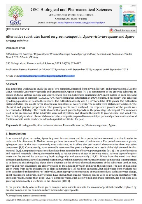
我种的会在紫外线下看见荧光的细菌!
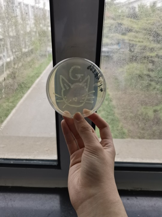
#daily#biotechnology#biology#ultraviolet#substrates#technology#school#high school#cat#school life#interesting#expectations#bacteria#flsorescence#fluorescences#experiment#inedible#pcr#genetically modified#my photos
1 note
·
View note
Text
Introducing iNPACK™ Our Miniaturization Solutions Business Unit. Specializing in Organic Substrates & Advanced Packaging Check out our recent customer conference video at PCB Technologies!
It was a huge success, showcasing our capabilities and expertise in miniaturization, substrate production, and more. Over 140 professionals attended and the level of engagement was outstanding.
We have gone from a mini-manufacturer to a full-full-fielded development center for our customers and received valuable feedback reinforcing our company's worth.
https://www.pcb-technologies.com/
#pcbdesign#packaging#packagingdesign#BeyondDesignLimits#pcb assembly services#pcb fabrication#PCB#reliabilityengineering#microelectronics#QTA#sip#substrates#miniaturization
0 notes
Text

The burning shadows of human hands are
far too much for a single life
The things I see are a dread I must withstand.
Arthur and the King in Yellow
#arthur lester#malevolent#arthur malevolent#king in yellow#king in yellow malevolent#malevolent podcast#malevolent pod#malevolent arthur#arthur lester malevolent#malevolent king in yellow#kiy malevolent#anyway they are like tropical fish to me [colors i can barely see because i am red green colorblind]#we should get the eldritch creature trio (yellow john and king) and put them in a terrarium filled with rocks#so i can observe their behaviors like they are exotic lizards#arthurs in there too but he keeps getting stuck in the substrate#my art#AHH I FORGOT TO TAG the lyrics are the song Uncanny by GHOST
589 notes
·
View notes
Photo
precious cargo
#mine#original#OUGH hello....im tired#i see to have no time...so sad so tragic#i finished reading a book yesterday called th goblin emperor and KSBDGKDKSJKDGB#HELLO??? HELLO???#love love love love love love love#brain worms#maia..........omg...#im like rationing th other 2 books by reading a mediocre fantasy#im sleeby...im stiff....im gna...have a bath...hehehehehe#also isopods r arriving on >:) wednesday >:) hehehHEHEH#i hve their box...i got some hides.....waiting on my substrate n the BUGS
3K notes
·
View notes
Note
Can paper towel be an okay substrate for a snake long-term?
Paper towel is generally best as a short-term substrate, for when a snake is in quarantine or you need to keep a very close eye on their waste for whatever reason.
More natural substrates run circles around paper towel in almost every category, really. It's easier for snakes to perform natural behaviors, but you also have to swap out paper towel at least once a week, whereas if you're diligent about spot-cleaning, you can go months between deep cleans with natural substrates.
I only have a couple snakes that I keep on paper towel long-term for whatever reason, and it's just so inconvenient compared to other substrates. One snake I keep on paper towel (at least until he's at least two years old and has a stronger immune system) is my Mexican black kingsnake Ed, and I keep him on paper towel because he had a very persistent recurring tooth infection as a baby, so he needs to be eating in very sterile conditions and I need to know ASAP if there are any irregularities with his bowel movements. Even though it's necessary for him right now, I can't wait to change it because he's a very messy eater (in typical kingsnake fashion) and I feel like I have to change the towels at least a few times a week.
That's probably why it's so hard for me to get good pictures of him, now that I think about it - like every picture I get of Ed looks like this. Little black snake + paper towels that he likes to hide under = bad pictures.
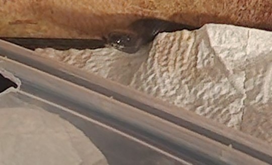
133 notes
·
View notes
Note
Kammerzell 2005 had a theory that Old Ægyptian has many pairs of synonyms, where one is Afro-Asiatic, while the other is para-IE
which sounds like bullshit

Oh fun, I think I've noticed one or two of these too; but yes a bunch of others immediately look like stretches, say, *ter- seems to mean primarily 'weak', only secondarily from there 'young creature', and specific 'child' only in a few still more derived reflexes like in Ossetic and Albanian.
I could imagine an IE loan stratum getting into Egyptian circa Sea Peoples; but also bare CC (or even single C!) root comparisons with PIE are a bit too easy to find, especially if we're apparently getting them from Pokorny instead of e.g. keeping any track of laryngeals.
13 notes
·
View notes
Text


@rottenrichi gave me a vision
#finished stuff#welcome home#frank welcome home#howdy welcome home#frank frankly#howdy pillar#the box is going to be his substrate food and enrichment
223 notes
·
View notes
Text

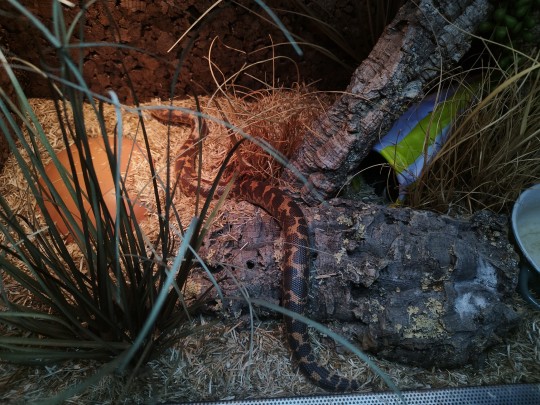
the man of the sand!!!!
#i changed his substrate so he for once is uprooted and exposed#he is 6-7 years now. such a good guy#kenyan sandboa#dw i filled the water bowl after taking the pics it was just empty for cleaning reasons
86 notes
·
View notes
Text


4 March 2024
First day of thesis work aaaa!
It actually wasn't that exciting in terms of the lab work I got to do, but it was exciting in terms of... everything else lol. I did the first synthesis and left the whole thing to crystallize (thesis supervisor said to forget about the solutions - apparently, they crystallize better when you aren't thinking about them ahaha). The entire day was a great challenge for my social anxiety and I'm very happy with how I handled things :) I'm exhausted though. I think I'll sleep supremely well tonight
#also can you see my substrate in the beaker in the second pic#isn't it pretty!#erbium compunds are often cute like that#mine#studyblr#chemblr#studyspo#study motivation#thesis tag
108 notes
·
View notes
Text
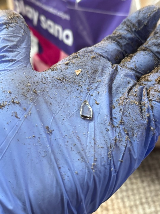
Reminder to everyone that uses a sand/soil mix as substrate for their reptiles to very carefully check through as you’re mixing 😐
I don’t even know if this came from the soil or sand. I’m inclined to think soil, but I genuinely do not know.
#psa#nearly enough to make me angrily switch back to lignocel but I really don’t want to ugh#plus I don’t have any in my house rn#Jesus fuck#know what would be great? your snake being fucking gutted on their substrate
66 notes
·
View notes
Last Seen Blogs

anomaliata
Complete Irregularity

detroit-become-hurt
Multifandom Imagines

goldensadnessdolphin
GoldenSadnessDolphin

superssaralance
Untitled

thefirst-one
The Blip